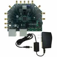
AD9272-65EBZ Analog Devices Inc, AD9272-65EBZ Datasheet
AD9272-65EBZ
Specifications of AD9272-65EBZ


Related parts for AD9272-65EBZ


AD9272-65EBZ Summary of contents
Page 1
... Medical imaging/ultrasound Automotive radar GENERAL DESCRIPTION The AD9272 is designed for low cost, low power, small size, and ease of use. It contains eight channels of a low noise preamplifier (LNA) with a variable gain amplifier (VGA), an antialiasing filter (AAF), and a 12-bit, 10 MSPS to 80 MSPS analog-to- digital converter (ADC) ...
Page 2
... AD9272 TABLE OF CONTENTS Features .............................................................................................. 1 Applications ....................................................................................... 1 General Description ......................................................................... 1 Functional Block Diagram .............................................................. 1 Revision History ............................................................................... 2 Product Highlights ........................................................................... 3 Specifications ..................................................................................... 4 AC Specifications .......................................................................... 4 Digital Specifications ................................................................... 8 Switching Specifications .............................................................. 9 Absolute Maximum Ratings .......................................................... 11 Thermal Impedance ................................................................... 11 ESD Caution ................................................................................ 11 Pin Configuration and Function Descriptions ........................... 12 Typical Performance Characteristics ........................................... 15 Equivalent Circuits ......................................................................... 19 Theory of Operation ...................................................................... 21 REVISION HISTORY 7/09— ...
Page 3
... Fabricated in an advanced CMOS process, the AD9272 is available × 16 mm, RoHS-compliant, 100-lead TQFP specified over the industrial temperature range of −40°C to +85°C. ...
Page 4
... Rev Page Ω, LNA gain = 21.3 dB, LNA bias = high, S AD9272-80 Max Min Typ Max 15.6/17.9/21.3 9.6/11.9/15.3 dB 733/550/367 0.9 50 100 15 22 100 0.98/0.86/0.75 1 1.0/0.8/0.5 4.8/4.0/3.2 dB 3.4/2.8/2 and ± ...
Page 5
... Rev Page AD9272 AD9272-80 Max Min Typ Max Unit ±2 ns 1.26/1.04/0.85 nV/√Hz 7.6/6.1/4.4 dB 4.5/3.6/2.7 dB −30 dB +35 −35 +35 LSB 63 dBFS 54.5 dBFS −55 dBc − ...
Page 6
... Rev Page AD9272-80 Max Min Typ Max Unit 1.5 dB +1.5 −1.6 +1.6 dB −2.5 dB +1.5 −1.6 +1.6 dB 0.1 dB 1.6 0 1.6 ...
Page 7
... Typ Max Min Typ 210 280 32 32 365 365 140 140 49 51 1560 1713 1690 475 475 5 175 1.6 1 ± Rev Page AD9272 AD9272-80 Max Min Typ Max Unit 335 365 mA 140 1860 1780 1975 mW 475 200 210 mW 1.6 mV/V 12 Bits ± ...
Page 8
... AD9272 DIGITAL SPECIFICATIONS AVDD1 = 1.8 V, AVDD2 = 3.0 V, DRVDD = 1.8 V, 1.0 V internal ADC reference, f Table 2. 1 Parameter CLOCK INPUTS (CLK+, CLK−) Logic Compliance 2 Differential Input Voltage Input Common-Mode Voltage Input Resistance (Differential) Input Capacitance LOGIC INPUTS (PDWN, STBY, SCLK) Logic 1 Voltage ...
Page 9
... FCO Full (t /24) − 300 (t SAMPLE SAMPLE Full (t /24) − 300 (t SAMPLE SAMPLE Full ±100 25°C 2 25°C 1 Full 8 25°C <1 Rev Page AD9272 Max Unit 80 MSPS ns ns /2) + 2.3 (t /2) + 3.1 ns SAMPLE ps ps /2) + 2.3 (t /2) + 3.1 ns SAMPLE /24) ns SAMPLE /24) (t /24) + 300 ...
Page 10
... AD9272 ADC Timing Diagrams N – 1 AIN t EH CLK– CLK+ t CPD DCO– DCO+ t FCO FCO– FCO DOUTx– DOUTx+ N – 1 AIN t EH CLK– CLK+ t CPD DCO– DCO+ t FCO FCO– FCO DOUTx– DOUTx FRAME t DATA MSB ...
Page 11
... PCB with a solid ground plane (simulated). The exposed JA −0 +2.0 V pad is soldered to the PCB. −0 +3.9 V ESD CAUTION −0 +2.0 V −0 +3.9 V −0 +2.0 V −40°C to +85°C −65°C to +150°C 150°C 300°C Rev Page AD9272 θ 1 θ θ Unit 20.3 N/A N/A °C/W 14.4 7 ...
Page 12
... LG-G 17 LO-H 18 LOSW-H 19 LI-H EXPOSED PADDLE, PIN 0 (BOTTOM OF PACKAGE) AD9272 TOP VIEW (Not to Scale) Figure 4. TQFP Pin Configuration Description Ground (exposed paddle should be tied to a quiet analog ground) 1.8 V Analog Supply 3.0 V Analog Supply 1.8 V Digital Output Driver Supply LNA Analog Input for Channel E ...
Page 13
... CW Doppler Output Complement for Channel 1 CW Doppler Output True for Channel 1 CW Doppler Output Complement for Channel 2 CW Doppler Output True for Channel 2 CW Doppler Output Complement for Channel 3 CW Doppler Output True for Channel 3 Gain Control Voltage Input Complement Rev Page AD9272 ...
Page 14
... AD9272 Pin No. Name 88 GAIN+ 89 RBIAS 90 VREF 91 CWD4− 92 CWD4+ 93 CWD5− 94 CWD5+ 95 CWD6− 96 CWD6+ 97 CWD7− 98 CWD7+ 99 LO-E 100 LOSW-E Description Gain Control Voltage Input True External Resistor to Set the Internal ADC Core Bias Current Voltage Reference Input/Output CW Doppler Output Complement for Channel 4 ...
Page 15
... Figure 8. Gain Error Histogram, GAIN –1.25 –1.00 –0.75 –0.50 –0.25 0 0.25 0.50 0.75 1.00 1.25 CHANNEL-TO-CHANNEL GAIN MATCHING (dB) Figure 9. Gain Match Histogram, GAIN –1.25 –1.00 –0.75 –0.50 –0.25 0 0.25 0.50 0.75 1.00 1.25 CHANNEL-TO-CHANNEL GAIN MATCHING (dB) Figure 10. Gain Match Histogram, GAIN+ = 1.3 V AD9272 ...
Page 16
... GAIN+ (V) Figure 15. SNR/SINAD vs. GAIN+, AIN = −1 dBFS 0 AD9272-65 –5 AD9272-80 –10 AD9272-40 –15 –20 – FREQUENCY (MHz) Figure 16. Antialiasing Filter (AAF) Pass-Band Response, LPF Cutoff = 1 × (1/4.5) × f SAMPLE LNA GAIN = 6× ...
Page 17
... GAIN GAIN+ = 0.8V –40 –35 –30 –25 –20 –15 –10 ADC OUTPUT LEVEL (dBFS 0.01MHz IN2 IN1 A = –1dBFS –21dBFS IN1 IN2 2.3MHz 5MHz 0.4 0.6 0.8 1.0 1.2 GAIN+ (V) Figure 22. IMD3 vs. GAIN+ AD9272 GAIN+ = 0.8V 0 GAIN+ = 1.6V –5 0 8MHz 1.4 1.6 ...
Page 18
... AD9272 5.00MHz, = 5.01MHz IN1 IN2 FUND2 LEVEL = FUND1 LEVEL – 20dB –20 –40 –60 GAIN –80 –100 GAIN+ = 0.8V –120 –40 –35 –30 –25 –20 –15 FUND1 LEVEL (dBFS) Figure 23. IMD3 vs. Fundamental 1 Amplitude Level GAIN+ = 1.6V –10 –5 0 Rev Page ...
Page 19
... Figure 26. Equivalent Clock Input Circuit AVDDx 1.25V Rev Page AVDDx 350Ω SDIO 30kΩ Figure 27. Equivalent SDIO Input Circuit DRVDD V V DOUTx– DOUTx DRGND Figure 28. Equivalent Digital Output Circuit 1kΩ SCLK, PDWN, OR STBY 30kΩ Figure 29. Equivalent SCLK, PDWN, or STBY Input Circuit AD9272 ...
Page 20
... AD9272 100Ω RBIAS Figure 30. Equivalent RBIAS Circuit AVDDx 70kΩ 1kΩ CSB Figure 31. Equivalent CSB Input Circuit VREF 6kΩ Figure 32. Equivalent VREF Circuit AVDDx Rev Page AVDD2 50Ω GAIN+ Figure 33. Equivalent GAIN+ Input Circuit 40Ω GAIN– +0.5V Figure 34. Equivalent GAIN− Input Circuit 10Ω ...
Page 21
... THEORY OF OPERATION ULTRASOUND The primary application for the AD9272 is medical ultrasound. Figure 36 shows a simplified block diagram of an ultrasound system. A critical function of an ultrasound system is the time gain control (TGC) compensation for physiological signal attenuation. Because the attenuation of ultrasound signals is exponential with respect to distance (time), a linear-in-dB VGA is the optimal solution ...
Page 22
... LNA. This V – O generally shows offset voltage that can vary from LOSW-x channel to channel and part to part given the application and LO-x layout of the PCB (see Figure 38 LG Rev Page CWD[7:0]+ CWD[7:0]– DOUTx+ SERIAL PIPELINE FILTER LVDS ADC DOUTx– AD9272 ...
Page 23
... Table 7 IN and C in terms because the dc levels at Pin LO-x FB Minimum R (Ω) R (Ω) C (pF 200 90 50 250 70 50 350 50 100 400 30 100 500 20 100 700 10 200 800 N/A 200 1000 N/A 200 1400 N/A AD9272 100M FB should (MHz ...
Page 24
... AD9272 LNA Noise The short-circuit noise voltage (input-referred noise impor- tant limit on system performance. The short-circuit input-referred noise voltage for the LNA is 0.85 nV/√ gain of 21.3 dB, including the VGA noise at a VGA postamp gain of 27 dB. These measurements, which were taken without a feedback resistor, provide the basis for calculating the input noise and noise figure (NF) performance of the configurations shown in Figure 40 ...
Page 25
... Register 0x2C (see Table 17) to connect to the noninverting AD9272 output to provide a differential output of the LNA. The LNA output 10nF full-scale voltage of the AD9272 is 4.4 V p-p, and the input full- LNA scale voltage is 2 attenuation is provided between 10nF the LNA output and the demodulator, the LNA input full-scale voltage must be limited ...
Page 26
... CHANNEL g LNA m g LNA m Figure 44. Typical Connection Interface with the AD8333 or AD8339 Using the CWDx± Outputs AD9272 LNA LNA LNA Figure 45. Typical Connection Interface with the AD8333 or AD8339 Using the LO-x and LOSW-x Outputs 600µH 2.5V 700Ω ...
Page 27
... The maximum number of channels combined must be considered when setting the load impedance for current-to-voltage conversion to ensure that the full-scale swing and common-mode voltage are within the operating limits of the AD9272. When interfacing to the AD8339, a common-mode voltage of 2.5 V and a full-scale swing of 2.8 V p-p are desired. This can be accomplished by connecting an inductor between each CWD output and a 2 ...
Page 28
... AD9272 Table 9. Sensitivity and Dynamic Range of Trade-Offs LNA Gain Input-Referred Full-Scale Input Noise Voltage (V p-p) (nV/√Hz) (V/V) (dB) 6 15.6 0.733 0.98 8 17.9 0.550 0.86 12 21.3 0.367 0.75 1 LNA: output full scale = 4.4 V p-p differential. 2 Filter: loss ~ 1 dB, NBW = 13.3 MHz, GAIN− = 0.8 V. ...
Page 29
... Figure 52. In either method, the GAIN+ and GAIN− pins should be dc-coupled and driven to accom- modate a 1.6 V full-scale input. – POSTAMP Rev Page AD9272 100Ω GAIN+ 0.01µF 50Ω GAIN– KELVIN 0.01µF CONNECTION Figure 51. Single-Ended GAIN± Pins Configuration AD9272 GAIN 0V TO 1.6V DC ...
Page 30
... AD9272 499Ω AD9272 ±0.4DC AT 100Ω 0.8V CM GAIN+ 0.01µF 0.8V CM AD8138 100Ω GAIN– ±0.4DC AT 0.01µF 0.8V CM 499Ω Figure 52. Differential GAIN± Pins Configuration VGA Noise In a typical application, a VGA compresses a wide dynamic range input signal to within the input span of an ADC. The ...
Page 31
... AD9272 to approximately 0.8 V p-p differential. This helps prevent the large voltage swings of the clock from feeding through to other portions of the AD9272, and it preserves the fast rise and fall times of the signal, which are critical to low jitter performance. ...
Page 32
... ANALOG INPUT FREQUENCY (MHz) Figure 59. Ideal SNR vs. Analog Input Frequency and Jitter Power Dissipation and Power-Down Mode As shown in Figure 61, the power dissipated by the AD9272 is proportional to its sample rate. The digital power dissipation does not vary much because it is determined primarily by the DRVDD supply and bias current of the LVDS output drivers ...
Page 33
... The AD9272 returns to normal operating mode when the PDWN pin is pulled low. This pin is both 1.8 V and 3.3 V tolerant. By asserting the STBY pin high, the AD9272 is placed into a standby mode. In this state, the device typically dissipates 150 mW. During standby, the entire part is powered down except the internal references ...
Page 34
... AD9272 600 EYE: ALL BITS 400 200 100 0 –100 –200 –400 –600 –1.5ns –1.0ns –0.5ns 0ns –200ps –100ps 0ps Figure 64. Data Eye for LVDS Outputs in ANSI-644 Mode with Trace Lengths of Less Than 24 Inches On Standard FR-4 ULS: 2398/2398 0.5ns 1.0ns 1.5ns 100ps 200ps Figure 65 ...
Page 35
... See Table 17 for details on enabling this feature. Two output clocks are provided to assist in capturing data from the AD9272. DCO± is used to clock the output data and is equal to six times the sampling clock rate. Data is clocked out of the AD9272 and must be captured on the rising and falling edges of the DCO± ...
Page 36
... When applying the decoupling capacitors to the VREF pin, use ceramic low-ESR capacitors. These capacitors should be close to the reference pin and on the same layer of the PCB as the AD9272. The VREF pin should have both a 0.1 μF capacitor and a 1 μF capacitor connected in parallel to the analog ground. These capacitor values are recommended for the ADC to properly settle and acquire the next valid sample ...
Page 37
... This ensures several tie points between the two during the reflow process. Using one continuous plane with no partitions only guarantees one tie point between the AD9272 and PCB. See Figure 67 for a PCB layout example. For more detailed infor- mation on packaging and for more PCB layout examples, see the AN-772 Application Note ...
Page 38
... The pins described in Table 15 constitute the physical interface between the programming device of the user and the serial port of the AD9272. The SCLK and CSB pins function as inputs when using the SPI interface. The SDIO pin is bidirectional, functioning as an input during write phases and as an output during readback ...
Page 39
... Minimum time for the SDIO pin to switch from an input to an output relative to the SCLK falling edge (not shown in Figure 69) Minimum time for the SDIO pin to switch from an output to an input relative to the SCLK rising edge (not shown in Figure 69) Rev Page DON’T CARE AD9272 DON’T CARE ...
Page 40
... AD9272 MEMORY MAP READING THE MEMORY MAP TABLE Each row in the memory map table has eight address locations. The memory map is roughly divided into three sections: the chip configuration register map (Address 0x00 to Address 0x02), the device index and transfer register map (Address 0x04 to Address 0xFF), and the ADC functions register map (Address 0x08 to Address 0x2D) ...
Page 41
... Table 17. AD9272 Memory Map Register Addr. Bit 7 (Hex) Register Name (MSB) Bit 6 Chip Configuration Registers 00 Chip_port_config 0 LSB first off (default) 01 Chip_id 02 Chip_grade X X Device Index and Transfer Registers 04 Device_index_2 Device_index_1 device_update X X ADC Functions 08 Modes Clock Test_io User test mode 00 = off (default) ...
Page 42
... AD9272 Addr. Bit 7 (Hex) Register Name (MSB) Bit 6 0F Flex_channel_input Filter cutoff frequency control 0000 = 1.3 × 1/3 × f 0001 = 1.2 × 1/3 × f 0010 = 1.1 × 1/3 × f 0011 = 1.0 × 1/3 × f 0100 = 0.9 × 1/3 × f 0101 = 0.8 × 1/3 × f 0110 = 0.7 × ...
Page 43
... CWD1− (single-ended) 11 1010 = CWD2− (single-ended) 11 1011 = CWD3− (single-ended) 11 1100 = CWD4− (single-ended) 11 1101 = CWD5− (single-ended) 11 1110 = CWD6− (single-ended) 11 1111 = CWD7− (single-ended) 0x xxxx = power down CW channel (default) Rev Page AD9272 Bit 0 Default Default Notes/ Bit 1 (LSB) Value Comments B1 ...
Page 44
... AD9272BSVZRL-65 −40°C to +85°C 1 AD9272BSVZ-40 −40°C to +85°C 1 AD9272BSVZRL-40 −40°C to +85°C 1 AD9272-65EBZ 1 AD9272-80KITZ RoHS Compliant Part. ©2009 Analog Devices, Inc. All rights reserved. Trademarks and registered trademarks are the property of their respective owners. 16.00 BSC SQ 14.00 BSC SQ ...