EVAL-AD7767-1EDZ Analog Devices Inc, EVAL-AD7767-1EDZ Datasheet - Page 20
EVAL-AD7767-1EDZ
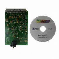
Manufacturer Part Number
EVAL-AD7767-1EDZ
Description
BOARD EVAL AD7767-1 64KSPS 111DB
Manufacturer
Analog Devices Inc
Specifications of EVAL-AD7767-1EDZ
Number Of Adc's
1
Number Of Bits
24
Sampling Rate (per Second)
64k
Data Interface
Serial
Inputs Per Adc
1 Differential
Input Range
±VREF
Power (typ) @ Conditions
10.5mW @ 64kSPS
Voltage Supply Source
Analog and Digital
Operating Temperature
-40°C ~ 105°C
Utilized Ic / Part
AD7767-1
Lead Free Status / RoHS Status
Lead free / RoHS Compliant


AD7767
DRIVING THE AD7767
The AD7767 must be driven with fully differential inputs. The
common-mode voltage of the differential inputs to the AD7767
device and therefore the limits on the differential inputs are set
by the reference voltage (V
mode voltage of the AD7767 is V
has a 5 V supply (using ADR445, ADR435, or ADR425), the
common mode is at 2.5 V, meaning that the maximum inputs that
can be applied on the AD7767 differential inputs are a 5 V p-p
input around 2.5 V.
An analog voltage of 2.5 V supplies the AD7767 AV
However, the AD7767 allows the user to apply a reference
voltage of up to 5 V. This provides the user with an increased
full-scale range, offering the user the option of using the
AD7767 with a greater LSB voltage. Figure 39 shows the
maximum inputs to the AD7767.
DIFFERENTIAL SIGNAL SOURCE
An example of recommended driving circuitry that can be used
in conjunction with the AD7767/AD7767-1/AD7767-2 is shown in
Figure 40. Figure 40 shows how the
used to drive an input to the AD7767/AD7767-1/AD7767-2
from a differential source. Each of the differential paths is
driven by an ADA4841-1 device.
SINGLE-ENDED SIGNAL SOURCE
For applications using a single-ended analog signal, either
bipolar or unipolar, the ADA4941-1 single-ended-to-differential
driver creates a fully differential input to the AD7767/AD7767-1/
AD7767-2. The schematic is shown in Figure 41.
Table 8. Resistor Values Required When Using the Differential to Single-Ended Circuit with ADA4941 (See Figure 41)
V
+20, −20
+10, −10
+5, −5
IN
(V)
Figure 39. Maximum Differential Inputs to the AD7767
V
V
V
V
V
2.5
2.5
2.5
0V
0V
REF
REF
REF
REF
2
2
OFFSET1
(V)
REF
) applied to the device. The common-
V
2.203
2.000
1.667
REF
OFFSET2
/2. When the AD7767 V
ADA4841-1
(V)
V
V
IN+
IN–
device can be
OUT+ (V)
−0.01, +4.96
0.01, 4.99
0.00, 5.00
DD
pin.
REF+
Rev. C | Page 20 of 24
pin
OUT− (V)
5.01, 0.04
4.99, 0.01
5.00, 0.00
R1 and R2 set the attenuation ratio between the input range and
the ADC range (V
the desired input resistance, signal bandwidth, antialiasing, and
noise contribution. The ratio of R2 to R1 should be equal to the
ratio of REF to the peak-to-peak input voltage. For example, for
the ±10 V range with a 4 kΩ impedance, R2 = 1 kΩ and R1 = 4 kΩ.
R3 and R4 set the common mode on the IN− input, and R5 and R6
set the common mode on the IN+ input of the ADC. The common
mode, which is equal to the voltage present at V
close to V
ratio of V
AIN+
*SEE V
AIN–
Vin
REFERENCE
R5
R3
VOLTAGE
100nF
100nF
REF+
Figure 40. Driving the AD7767 from a Fully Differential Source
R1
R1 (kΩ)
8.06
4.02
2
Voffset2
Figure 41. Driving the AD7767 from a Single-Ended Source
OFFSET1
INPUT SIGNAL SECTION FOR DETAILS.
REF
Voffset1
/2. The voltage present should roughly be set to the
1kΩ
1kΩ
1kΩ
1kΩ
to 1 + R2/R1.
FB
REF
IN
R6
R4
REF
R2 (kΩ)
1
1
1
). R1, R2, and C
–0.2V
5.2V
0.1µF
ADA4841-1
ADA4841-1
R2
C
F
ADA4941
3.3nF
3.3nF
1kΩ
1kΩ
OUTN
OUTP
V
IN
100µF
R4 (kΩ)
12.7
15
20
ADR445
ADR425
15Ω
15Ω
15Ω
15Ω
F
are chosen depending on
VOUT = 5V REF
2.2nF
2.2nF
0.1µF
R3 = R5 = R6 (kΩ)
10
10
10
2.2nF
2.2nF
OFFSET1
4
5
2.5V TO 5V
V
V
V
V
IN+
IN–
IN+
IN–
AGND
, should be
V
ADP3330-2.5
REF+
AD7767
AD7767
2.5V
ADR4xx
ADP3330-2.5
V
AV
DGND
REF+
1
2
DD
AV
LDO
2.5V
DD
*
Related parts for EVAL-AD7767-1EDZ
Image
Part Number
Description
Manufacturer
Datasheet
Request
R

Part Number:
Description:
IC, ADJ LDO REG, 1.5V TO 5V 250mA MSOP-8
Manufacturer:
Vishay
Datasheet:

Part Number:
Description:
IC, ADJ LDO REG, 1.5V TO 5V 0.6A 8-TSSOP
Manufacturer:
Vishay
Datasheet:
Part Number:
Description:
IC, ADJ LDO REG, 1.5V TO 5V 250mA MSOP-8
Manufacturer:
Vishay
Datasheet:

Part Number:
Description:
IC ADJ LDO REG 1.5V TO 5V 150mA 5-SOT-23
Manufacturer:
Vishay
Datasheet:

Part Number:
Description:
BOARD EVAL AS1324-AD
Manufacturer:
austriamicrosystems
Datasheet:
Part Number:
Description:
IC, ADJ LDO REG, 1.5V TO 5V 0.6A 8-TSSOP
Manufacturer:
Vishay
Datasheet:

Part Number:
Description:
IC, ADJ LDO REG, 1.5V TO 5V, 0.3A, MSOP8
Manufacturer:
Vishay
Datasheet:
Part Number:
Description:
IC, ADJ LDO REG, 1.5V TO 5V, 0.3A, MSOP8
Manufacturer:
Vishay
Datasheet:
Part Number:
Description:
IC, ADJ LDO REG 1.215V TO 5V 0.3A MSOP-8
Manufacturer:
Vishay
Datasheet:
Part Number:
Description:
IC, ADJ LDO REG 1.215V TO 5V 0.3A MSOP-8
Manufacturer:
Vishay
Datasheet:

Part Number:
Description:
±1.7g Dual-Axis IMEMS Accelerometer Evaluation Board
Manufacturer:
Analog Devices Inc
Datasheet:

Part Number:
Description:
IC MULTIPLIER ANALOG 8-SOIC T/R
Manufacturer:
Analog Devices Inc
Datasheet:

Part Number:
Description:
IC ANALOG MULTIPLIER 8-DIP
Manufacturer:
Analog Devices Inc
Datasheet:
Part Number:
Description:
IC ANALOG MULTIPLIER 8-SOIC
Manufacturer:
Analog Devices Inc
Datasheet:
Part Number:
Description:
IC ANALOG MULTIPLIER 8-DIP
Manufacturer:
Analog Devices Inc
Datasheet: