EVAL-AD7679CBZ Analog Devices Inc, EVAL-AD7679CBZ Datasheet - Page 8
EVAL-AD7679CBZ
Manufacturer Part Number
EVAL-AD7679CBZ
Description
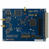
BOARD EVALUATION FOR AD7679
Manufacturer
Analog Devices Inc
Series
PulSAR®r
Specifications of EVAL-AD7679CBZ
Number Of Adc's
1
Number Of Bits
18
Sampling Rate (per Second)
570k
Data Interface
Serial, Parallel
Inputs Per Adc
1 Differential
Input Range
±VREF
Power (typ) @ Conditions
89mW @ 500kSPS
Voltage Supply Source
Analog and Digital
Operating Temperature
-40°C ~ 85°C
Utilized Ic / Part
AD7679
Lead Free Status / RoHS Status
Lead free / RoHS Compliant


AD7679
PIN CONFIGURATION AND FUNCTION DESCRIPTIONS
Table 6. Pin Function Descriptions
Pin No.
1, 44
2, 47
3
4
5
6, 7, 40–
42, 45
8
9
10
11, 12
Mnemonic
AGND
AVDD
MODE0
MODE1
D0/OB/2C
NC
D1/A0
D2/A1
D3
D[4:5]or
DIVSCLK[0:1]
Type
P
P
DI
DI
DI/O
DO
DI/O
DI/O
DI/O
1
Description
Analog Power Ground Pin.
Input Analog Power Pins. Nominally 5 V.
Data Output Interface Mode Selection.
Data Output Interface Mode Selection:
When MODE = 0 (18-bit interface mode), this pin is Bit 0 of the parallel port data output bus and the
data coding is straight binary. In all other modes, this pin allows choice of straight binary/binary twos
complement. When OB/2C is HIGH, the digital output is straight binary; when LOW, the MSB is
inverted, resulting in a twos complement output from its internal shift register.
No Connect.
When MODE = 0 (18-bit interface mode), this pin is Bit 1 of the parallel port data output bus. In all
other modes, this input pin controls the form in which data is output, as shown in Table 7.
When MODE = 0 or 1 (18-bit or 16-bit interface mode), this pin is Bit 2 of the parallel port data output
bus. In all other modes, this input pin controls the form in which data is output, as shown in Table 7.
In all modes except MODE = 3, this output is used as Bit 3 of the parallel port data output bus. This pin
is always an output, regardless of the interface mode.
In all modes except MODE = 3, these pins are Bit 4 and Bit 5 of the parallel port data output bus.
When MODE = 3 (serial mode), EXT/INT is LOW, and RDC/SDIN is LOW (serial master read after
convert), these inputs, part of the serial port, are used to slow down, if desired, the internal serial clock
that clocks the data output. In other serial modes, these pins are not used.
D4/DIVSCLK[0]
D5/DIVSCLK[1]
NOTES
1. NC = NO CONNECT.
2. THE EXPOSED PAD IS INTERNALLY CONNECTED TO AGND. THIS CONNECTION
Interface MODE
0
1
2
3
IS NOT REQUIRED TO MEET THE ELECTRICAL PERFORMANCES HOWEVER,
FOR INCREASED RELIABILITY OF THE SOLDER JOINTS, IT IS RECOMMENDED
THAT THE PAD BE SOLDERED TO THE ANALOG GROUND OF THE SYSTEM.
D0/OB/2C
MODE0
MODE1
AGND
D1/A0
D2/A1
AVDD
NC
NC
D3
10
11
12
1
2
3
4
5
6
7
8
9
48 47 46 45 44
13 14 15 16 17 18 19 20 21 22 23 24
PIN 1
IDENTIFIER
MODE1
0
0
1
1
Rev. A | Page 8 of 28
(Not to Scale)
AD7679
TOP VIEW
Figure 4.
43 42 41 40
MODE0
0
1
0
1
39 38 37
Description
18-Bit Interface
16-Bit Interface
Byte Interface
Serial Interface
36
35
34
33
32
31
30
29
28
27
26
25
AGND
CNVST
PD
RESET
CS
RD
DGND
BUSY
D17
D16
D15
D14
Related parts for EVAL-AD7679CBZ
Image
Part Number
Description
Manufacturer
Datasheet
Request
R


Part Number:
Description:
BOARD EVAL FOR SI270X-A
Manufacturer:
Silicon Laboratories Inc
Datasheet:

Part Number:
Description:
BUCK CONV REF DESIGN KIT IP1201
Manufacturer:
International Rectifier
Datasheet:
Part Number:
Description:
BOARD DEMO SYNC DUAL BUCK CNVTER
Manufacturer:
International Rectifier
Datasheet:
Part Number:
Description:
BOARD DEMO SYNC BUCK CONVETER
Manufacturer:
International Rectifier
Datasheet:

Part Number:
Description:
EVALBOARD/EB Omnidirectional microphone - Analog
Manufacturer:
Analog Devices
Datasheet:
Part Number:
Description:
EVALBOARD/EB Omnidirectional microphone - Analog
Manufacturer:
Analog Devices
Datasheet:


Part Number:
Description:
BOARD EVAL LED DRIVER LT3756
Manufacturer:
Linear Technology
Datasheet:

Part Number:
Description:
BOARD EVAL FOR AD7741/7742
Manufacturer:
Analog Devices Inc
Datasheet:

Part Number:
Description:
±1.7g Dual-Axis IMEMS Accelerometer Evaluation Board
Manufacturer:
Analog Devices Inc
Datasheet:

Part Number:
Description:
IC MULTIPLIER ANALOG 8-SOIC T/R
Manufacturer:
Analog Devices Inc
Datasheet:

Part Number:
Description:
IC ANALOG MULTIPLIER 8-DIP
Manufacturer:
Analog Devices Inc
Datasheet:
Part Number:
Description:
IC ANALOG MULTIPLIER 8-SOIC
Manufacturer:
Analog Devices Inc
Datasheet:
Part Number:
Description:
IC ANALOG MULTIPLIER 8-DIP
Manufacturer:
Analog Devices Inc
Datasheet: