EVAL-AD7730EBZ Analog Devices Inc, EVAL-AD7730EBZ Datasheet - Page 4
EVAL-AD7730EBZ
Manufacturer Part Number
EVAL-AD7730EBZ
Description
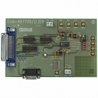
BOARD EVAL FOR AD7730
Manufacturer
Analog Devices Inc
Datasheet
1.EVAL-AD7730EBZ.pdf
(8 pages)
Specifications of EVAL-AD7730EBZ
Number Of Adc's
1
Number Of Bits
24
Sampling Rate (per Second)
1.2k
Data Interface
Serial
Inputs Per Adc
2 Differential
Input Range
±80 mV
Power (typ) @ Conditions
125mW @ 1.2kSPS
Voltage Supply Source
Analog and Digital
Operating Temperature
-40°C ~ 85°C
Utilized Ic / Part
AD7730
Lead Free Status / RoHS Status
Lead free / RoHS Compliant
Other names
EVAL-AD7730EB
EVAL-AD7730EB
EVAL-AD7730EB


EVAL-AD7730EB
1
2
3
4
5
6
7-8
9
10
11-12
13
14-18
19-30
31-36
NC
DIN
RESET
CS
SCLK
SYNC
NC
DV
RDY
NC
DOUT
NC
DGND
NC
DD
36
18
No Connect. This pin is not connected on the evaluation board.
Serial Data Input. Data applied to this pin is buffered before being applied to the AD7730's DIN pin. The
serial data applied to the DIN pin is written to the input shift register on the part. Data from this input shift
register is transferred to one of the on-chip registers depending on the register selection bits of the
Communications Register.
Reset Input. The signal on this pin is buffered before being applied to the RESET pin of the AD7730.
RESET is an active low input which resets the control logic, interface logic, calibration coefficients, digital
filter and all on-chip registers to power-on status.
Chip Select. The signal on this pin is buffered before being applied to the CS pin of the AD7730. CS is an
active low logic input used to select the AD7730. With this input hard-wired low, the AD7730 operates in its
three-wire interface mode with SCLK, DIN and DOUT used to interface to the device. CS can be used to
select the device in systems with more than one device on the serial bus or as a frame synchronisation signal
in communicating with the AD7730.
Serial Clock. The signal on this pin is buffered before being applied to the SCLK pin of the AD7730. An
external serial clock is applied to this input to access serial data from the AD7730. This serial clock can be a
continuous clock with all data transmitted in a continuous train of pulses. Alternatively, it can be a non-con-
tinuous clock with the information being transmitted to the AD7730 in smaller batches of data.
Logic Input. The signal on this pin is buffered before being applied to the SYNC pin of the AD7730. The
SYNC input allows for synchronisation of the digital filters and analog modulators across a number of
AD7730s. While SYNC is low, the nodes of the digital filter, the filter control logic, and the calibration con-
trol logic are reset and the analog modulator is also held in its reset state.
No Connect. These pins are not connected on the evaluation board.
Digital Supply Voltage. This provides the supply voltage for IC4, the buffer chip which buffers the output
signals from the AD7730 before they are applied to SKT2.
Logic output. This is a buffered version of the signal on the AD7730's RDY pin. RDY is used as a status
output in both conversion and calibration mode. In conversion mode, a logic low on the RDY output indi-
cates that a new output word is available from the AD7730 data register. The RDY pin will return high upon
completion of a read operation of a full output word. If no data read has taken place after an output update,
the RDY line will return high prior to the next output update, remain high while the update is taking place
and return low again. This gives an indication of when a read operation should not be initiated to avoid
reading from the data register as it is being updated. In calibration mode, RDY goes high when calibration is
initiated and returns low to indicate that calibration is complete.
No Connect. These pins are not connected on the evaluation board.
Serial Data Output. This is a buffered version of the signal on the AD7730's DOUT pin. Serial data from
the output shift register on the part is clocked out on this pin. This output shift register contains information
from one of the nine on-chip registers depending on the register selection bits of the Communications
Register.
No Connect. These pins are not connected on the evaluation board.
Ground reference point for digital circuitry. Connects to the DGND plane on the evaluation board.
No Connect. These pins are not connected on the evaluation board.
Table III. SKT2 Pin Designations
Figure 3. SKT2 Pin Configuration
–4–
19
1
REV. A
Related parts for EVAL-AD7730EBZ
Image
Part Number
Description
Manufacturer
Datasheet
Request
R


Part Number:
Description:
BOARD EVAL FOR SI270X-A
Manufacturer:
Silicon Laboratories Inc
Datasheet:

Part Number:
Description:
BUCK CONV REF DESIGN KIT IP1201
Manufacturer:
International Rectifier
Datasheet:
Part Number:
Description:
BOARD DEMO SYNC DUAL BUCK CNVTER
Manufacturer:
International Rectifier
Datasheet:
Part Number:
Description:
BOARD DEMO SYNC BUCK CONVETER
Manufacturer:
International Rectifier
Datasheet:

Part Number:
Description:
EVALBOARD/EB Omnidirectional microphone - Analog
Manufacturer:
Analog Devices
Datasheet:
Part Number:
Description:
EVALBOARD/EB Omnidirectional microphone - Analog
Manufacturer:
Analog Devices
Datasheet:


Part Number:
Description:
BOARD EVAL LED DRIVER LT3756
Manufacturer:
Linear Technology
Datasheet:

Part Number:
Description:
BOARD EVAL FOR AD7741/7742
Manufacturer:
Analog Devices Inc
Datasheet:

Part Number:
Description:
±1.7g Dual-Axis IMEMS Accelerometer Evaluation Board
Manufacturer:
Analog Devices Inc
Datasheet:

Part Number:
Description:
IC MULTIPLIER ANALOG 8-SOIC T/R
Manufacturer:
Analog Devices Inc
Datasheet:

Part Number:
Description:
IC ANALOG MULTIPLIER 8-DIP
Manufacturer:
Analog Devices Inc
Datasheet:
Part Number:
Description:
IC ANALOG MULTIPLIER 8-SOIC
Manufacturer:
Analog Devices Inc
Datasheet:
Part Number:
Description:
IC ANALOG MULTIPLIER 8-DIP
Manufacturer:
Analog Devices Inc
Datasheet: