EVAL-AD7794EBZ Analog Devices Inc, EVAL-AD7794EBZ Datasheet - Page 24
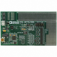
EVAL-AD7794EBZ
Manufacturer Part Number
EVAL-AD7794EBZ
Description
BOARD EVALUATION FOR AD7794
Manufacturer
Analog Devices Inc
Specifications of EVAL-AD7794EBZ
Number Of Adc's
1
Number Of Bits
24
Sampling Rate (per Second)
470
Data Interface
SPI™, QSPI™, MICROWIRE™, and DSP
Inputs Per Adc
6 Differential
Input Range
±VREF/gain
Power (typ) @ Conditions
2.5mW @ 470SPS
Voltage Supply Source
Analog and Digital
Operating Temperature
-40°C ~ 105°C
Utilized Ic / Part
AD7794
Lead Free Status / RoHS Status
Lead free / RoHS Compliant


AD7794/AD7795
DATA REGISTER
RS2, RS1, RS0 = 0, 1, 1; Power-On/Reset =
0x0000(AD7795), 0x000000 (AD7794)
The conversion result from the ADC is stored in this data
register. This is a read-only register. On completion of a read
operation from this register, the RDY bit/pin is set.
ID REGISTER
RS2, RS1, RS0 = 1, 0, 0; Power-On/Reset = 0xXF
The identification number for the AD7794/AD7795 is stored in
the ID register. This is a read-only register.
IO7
0(0)
Table 21. IO Register Bit Designations
Bit No.
IO7
IO6
IO5 to IO4
IO3 to IO2
IO3 to IO2
IO6
IOEN(0)
0
Mnemonic
IOEN
IO2DAT/IO1DAT
IEXCDIR1 to IEXCDIR0
IEXCEN1 to IEXCEN0
IO5
IO2DAT(0)
Description
This bit must be programmed with a Logic 0 for correct operation.
Configures Pin AIN6(+)/P1 and Pin AIN6(−)/P2 as analog input pins or digital output pins. When this
bit is set, the pins are configured as Digital Output Pin P1 and Digital Output Pin P2. When this bit is
cleared, these pins are configured as Analog Input Pin AIN6(+) and Analog Input Pin AIN6(−).
P2/P1 Data. When IOEN is set, the data for Digital Output Pin P1 and Digital Output Pin P2 is written
to Bit IO2DAT and Bit IO1DAT.
Direction of Current Sources Select Bits.
IEXCDIR1
0
0
1
1
These bits are used to enable and disable the current sources. They also select the value of the
excitation currents.
IEXCEN1
0
0
1
1
IO4
IO1DAT(0)
IEXCDIR0
0
1
0
1
IEXCEN0
0
1
0
1
Rev. D | Page 24 of 36
IO3
IEXCDIR1(0)
Current Source Direction
Current Source IEXC1 connected to Pin IOUT1. Current Source IEXC2
connected to Pin IOUT2.
Current Source IEXC1 connected to Pin IOUT2. Current Source IEXC2
connected to Pin IOUT1.
Both current sources connected to Pin IOUT1. Permitted only when the
current sources are set to 10 μA or 210 μA.
Both current sources connected to Pin IOUT2. Permitted only when the
current sources are set to 10 μA or 210 μA.
Current Source Value
Excitation currents disabled
10 μA
210 μA
1 mA
IO REGISTER
RS2, RS1, RS0 = 1, 0, 1; Power-On/Reset = 0x00
The IO register is an 8-bit read/write register that is used
to enable the excitation currents and select the value of the
excitation currents.
Table 21 outlines the bit designations for the IO register. IO0
through IO7 indicate the bit locations. IO denotes that the bits
are in the IO register. IO7 denotes the first bit of the data
stream. The number in brackets indicates the power-on/reset
default status of that bit.
IO2
IEXCDIR0(0)
IO1
IEXCEN1(0)
IO0
IEXCEN0(0)
Related parts for EVAL-AD7794EBZ
Image
Part Number
Description
Manufacturer
Datasheet
Request
R


Part Number:
Description:
BOARD EVAL FOR SI270X-A
Manufacturer:
Silicon Laboratories Inc
Datasheet:

Part Number:
Description:
BUCK CONV REF DESIGN KIT IP1201
Manufacturer:
International Rectifier
Datasheet:
Part Number:
Description:
BOARD DEMO SYNC DUAL BUCK CNVTER
Manufacturer:
International Rectifier
Datasheet:
Part Number:
Description:
BOARD DEMO SYNC BUCK CONVETER
Manufacturer:
International Rectifier
Datasheet:

Part Number:
Description:
EVALBOARD/EB Omnidirectional microphone - Analog
Manufacturer:
Analog Devices
Datasheet:
Part Number:
Description:
EVALBOARD/EB Omnidirectional microphone - Analog
Manufacturer:
Analog Devices
Datasheet:


Part Number:
Description:
BOARD EVAL LED DRIVER LT3756
Manufacturer:
Linear Technology
Datasheet:

Part Number:
Description:
BOARD EVAL FOR AD7741/7742
Manufacturer:
Analog Devices Inc
Datasheet:

Part Number:
Description:
±1.7g Dual-Axis IMEMS Accelerometer Evaluation Board
Manufacturer:
Analog Devices Inc
Datasheet:

Part Number:
Description:
IC MULTIPLIER ANALOG 8-SOIC T/R
Manufacturer:
Analog Devices Inc
Datasheet:

Part Number:
Description:
IC ANALOG MULTIPLIER 8-DIP
Manufacturer:
Analog Devices Inc
Datasheet:
Part Number:
Description:
IC ANALOG MULTIPLIER 8-SOIC
Manufacturer:
Analog Devices Inc
Datasheet:
Part Number:
Description:
IC ANALOG MULTIPLIER 8-DIP
Manufacturer:
Analog Devices Inc
Datasheet: