CDB5529 Cirrus Logic Inc, CDB5529 Datasheet - Page 27
CDB5529
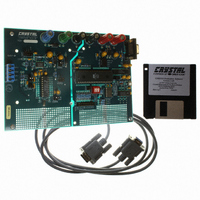
Manufacturer Part Number
CDB5529
Description
EVAL BOARD FOR CS5529
Manufacturer
Cirrus Logic Inc
Specifications of CDB5529
Number Of Adc's
1
Number Of Bits
16
Sampling Rate (per Second)
303
Data Interface
Serial
Inputs Per Adc
2 Differential
Input Range
±2.5 V
Power (typ) @ Conditions
2.6mW @ 2.5 V
Voltage Supply Source
Analog and Digital, Dual ±
Operating Temperature
-40°C ~ 85°C
Utilized Ic / Part
CS5529
Lead Free Status / RoHS Status
Contains lead / RoHS non-compliant
Other names
598-1015


A0, A1 - Logic Outputs (Analog), Pin 5, 6.
D0, D1, D2, D3 - Logic Outputs (Digital), Pin 7, 16, 17, 18.
Measurement and Reference Inputs
AIN+, AIN- - Differential Analog Input, Pins 3, 4.
VREF+, VREF- - Voltage Reference Input, Pins 20, 19.
Power Supply Connections
VA+ - Positive Analog Power, Pin 2.
VA- - Negative Analog Power, Pin 1.
VD+ - Positive Digital Power, Pin 13.
DGND - Digital Ground, Pin 12.
DS246F5
The logic states of A0-A1 mimic the states of the D22-D23 bits of the configuration register.
Logic Output 0 = VA-, and Logic Output 1 = VA+.
The logic states of D0-D3 mimic the states of the D18-D21 bits of the configuration register.
Logic Output 0 = DGND, and Logic Output 1 = VD+.
Differential input pins into the device.
Fully differential inputs which establish the voltage reference for the on-chip modulator.
Positive analog supply voltage.
Negative analog supply voltage.
Positive digital supply voltage (+3.0 V or +5 V).
Digital Ground.
CS5529
27
Related parts for CDB5529
Image
Part Number
Description
Manufacturer
Datasheet
Request
R

Part Number:
Description:
Development Kit
Manufacturer:
Cirrus Logic Inc
Datasheet:
Part Number:
Description:
Development Kit
Manufacturer:
Cirrus Logic Inc
Datasheet:


Part Number:
Description:
High-efficiency PFC + Fluorescent Lamp Driver Reference Design
Manufacturer:
Cirrus Logic Inc
Datasheet:
Part Number:
Description:
Development Kit
Manufacturer:
Cirrus Logic Inc
Datasheet:
Part Number:
Description:
Development Kit
Manufacturer:
Cirrus Logic Inc
Datasheet:

Part Number:
Description:
Development Kit
Manufacturer:
Cirrus Logic Inc
Datasheet:
Part Number:
Description:
Development Kit
Manufacturer:
Cirrus Logic Inc
Datasheet:
Part Number:
Description:
Development Kit
Manufacturer:
Cirrus Logic Inc
Datasheet:
Part Number:
Description:
Development Kit
Manufacturer:
Cirrus Logic Inc
Datasheet:

Part Number:
Description:
EVALUATION BOARD FOR CS8427
Manufacturer:
Cirrus Logic Inc
Datasheet:

Part Number:
Description:
BOARD EVAL FOR CS8416 RCVR
Manufacturer:
Cirrus Logic Inc
Datasheet:

Part Number:
Description:
EVALUATION BOARD FOR CS8420
Manufacturer:
Cirrus Logic Inc
Datasheet:

Part Number:
Description:
KIT DEVELOPMENT EP9315 ARM9
Manufacturer:
Cirrus Logic Inc
Datasheet:

Part Number:
Description:
KIT DEVELOPMENT EP9302 ARM9
Manufacturer:
Cirrus Logic Inc
Datasheet: