CDB5529 Cirrus Logic Inc, CDB5529 Datasheet - Page 15
CDB5529
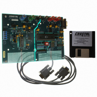
Manufacturer Part Number
CDB5529
Description
EVAL BOARD FOR CS5529
Manufacturer
Cirrus Logic Inc
Specifications of CDB5529
Number Of Adc's
1
Number Of Bits
16
Sampling Rate (per Second)
303
Data Interface
Serial
Inputs Per Adc
2 Differential
Input Range
±2.5 V
Power (typ) @ Conditions
2.6mW @ 2.5 V
Voltage Supply Source
Analog and Digital, Dual ±
Operating Temperature
-40°C ~ 85°C
Utilized Ic / Part
CS5529
Lead Free Status / RoHS Status
Contains lead / RoHS non-compliant
Other names
598-1015


Serial Port Initialization
The serial port is initialized to the command mode
whenever a power-on reset is performed or when
the port initialization sequence is completed. The
port initialization sequence involves clocking fif-
teen (or more) SYNC1 command bytes (0xFF) fol-
lowed by one SYNC0 command byte (0xFE). This
sequence places the chip in the command mode
where it waits until a valid command is received.
This function does not reset the internal registers to
their default settings. It only resets the serial port to
the command mode.
System Initialization
When power to the CS5529 is applied, the chip is
held in a reset condition until the 32.768 kHz oscil-
lator has started and a counter-timer elapses. Due to
the high Q of the 32.768 kHz crystal, the oscillator
takes 400-600 ms to start. The counter-timer counts
1002 oscillator clock cycles to make sure the oscil-
lator is fully stable. During this time-out period the
serial port logic is reset and the RV (Reset Valid)
bit in the configuration register is set to indicate
that a valid reset occurred. After a reset, the on-chip
registers are initialized to the following states and
the converter is placed in the command mode
where it waits for a valid command.
Note:
Configuration Register
The configuration register is a 24 bit register used
to modify the functions of the ADC. The following
sections detail the functions of the bits in the con-
figuration register.
DS246F5
Configuration Register:
Offset Register:
Gain Register:
A system reset can be initiated at any time by
writing a logic 1 to the RS (Reset System) bit
in the configuration register. After a reset, the
RV (Reset Valid) bit is set until the
configuration register is read. The user must
then write a logic 0 to the RS bit to take the
part out of the reset mode.
000040(H)
000000(H)
400000(H)
Latch Output Pins
The D3-D0 pins of the converter mimic the D21-
D18 bits of the configuration register. D3-D0 can
be used to control multiplexers and other digital
logic functions outside the converter. The D0-D3
outputs are powered from VD+ and DGND. Their
output voltage will be VD+ for a logic 1 and
DGND for a logic 0. The A1-A0 pins of the con-
verter mimic the D23-D22 bits of the configuration
register and can be used to control analog switches.
These outputs are powered from VA+ and VA-,
hence, their output voltage will be either VA+ for a
logic 1 or VA- for a logic 0.
All outputs can sink or source at least 1 mA, but it
is recommended to limit drive currents to less than
20 µA to reduce self-heating of the chip.
Power Consumption
The CS5529 accommodates four power consump-
tion modes: normal, low power, standby, and sleep.
The normal mode, the default mode, is entered after
a power-on-reset and typically consumes 2.5 mW.
The low power mode is an alternate mode that re-
duces the consumed power to 1.4 mW. It is entered
by setting bit D16 (the low power mode bit) in the
configuration register to logic 1. Since the convert-
er’s noise and linearity performance improves with
increased power consumption, slightly degraded
noise or linearity performance should be expected
in the low power mode.
The final two modes are the power save modes.
These modes power down most of the analog por-
tion of the chip and stop filter convolutions. The
power save modes are entered whenever the Power
Save (0x81 hexadecimal) command is issued to the
serial port. The particular power save mode entered
depends on state of bit D4 (the power save select
bit) in the configuration register. If D4 is logic 0,
the converter enters the standby mode reducing the
power consumption to 1 mW. The standby mode
leaves the oscillator and the on-chip bias generator
CS5529
15
Related parts for CDB5529
Image
Part Number
Description
Manufacturer
Datasheet
Request
R

Part Number:
Description:
Development Kit
Manufacturer:
Cirrus Logic Inc
Datasheet:
Part Number:
Description:
Development Kit
Manufacturer:
Cirrus Logic Inc
Datasheet:


Part Number:
Description:
High-efficiency PFC + Fluorescent Lamp Driver Reference Design
Manufacturer:
Cirrus Logic Inc
Datasheet:
Part Number:
Description:
Development Kit
Manufacturer:
Cirrus Logic Inc
Datasheet:
Part Number:
Description:
Development Kit
Manufacturer:
Cirrus Logic Inc
Datasheet:

Part Number:
Description:
Development Kit
Manufacturer:
Cirrus Logic Inc
Datasheet:
Part Number:
Description:
Development Kit
Manufacturer:
Cirrus Logic Inc
Datasheet:
Part Number:
Description:
Development Kit
Manufacturer:
Cirrus Logic Inc
Datasheet:
Part Number:
Description:
Development Kit
Manufacturer:
Cirrus Logic Inc
Datasheet:

Part Number:
Description:
EVALUATION BOARD FOR CS8427
Manufacturer:
Cirrus Logic Inc
Datasheet:

Part Number:
Description:
BOARD EVAL FOR CS8416 RCVR
Manufacturer:
Cirrus Logic Inc
Datasheet:

Part Number:
Description:
EVALUATION BOARD FOR CS8420
Manufacturer:
Cirrus Logic Inc
Datasheet:

Part Number:
Description:
KIT DEVELOPMENT EP9315 ARM9
Manufacturer:
Cirrus Logic Inc
Datasheet:

Part Number:
Description:
KIT DEVELOPMENT EP9302 ARM9
Manufacturer:
Cirrus Logic Inc
Datasheet: