CDB5345 Cirrus Logic Inc, CDB5345 Datasheet - Page 25
CDB5345
Manufacturer Part Number
CDB5345
Description
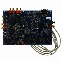
EVALUATION BOARD FOR CS5345
Manufacturer
Cirrus Logic Inc
Specifications of CDB5345
Number Of Adc's
2
Number Of Bits
24
Sampling Rate (per Second)
192k
Data Interface
Serial
Inputs Per Adc
6 Single Ended
Power (typ) @ Conditions
400mW @ 5 V
Voltage Supply Source
Analog and Digital
Operating Temperature
-10°C ~ 70°C
Utilized Ic / Part
CS5345
Description/function
Audio A/D
Operating Supply Voltage
5 V
Product
Audio Modules
For Use With/related Products
CS5345
Lead Free Status / RoHS Status
Contains lead / RoHS non-compliant
Lead Free Status / RoHS Status
Lead free / RoHS Compliant, Contains lead / RoHS non-compliant
Other names
598-1780


DS658F2
4.4
4.5
4.6
Analog Input Multiplexer, PGA, and Mic Gain
The CS5345 contains a stereo 6-to-1 analog input multiplexer followed by a programmable gain amplifier
(PGA). The input multiplexer can select one of six possible stereo analog input sources and route it to the
PGA. Analog inputs 4A and 4B are able to insert a +32 dB gain stage before the input multiplexer, allowing
them to be used for microphone-level signals without the need for any external gain. The PGA stage pro-
vides ±12 dB of gain or attenuation in 0.5 dB steps.
PGA, and microphone gain stages.
The
multiplexer and mic gain.
- Address 08h” on page 34
level input 1 is selected, and the PGA is set to 0 dB.
Input Connections
The analog modulator samples the input at 6.144 MHz (MCLK=12.288 MHz). The digital filter will reject sig-
nals within the stopband of the filter. However, there is no rejection for input signals which are
(n
for the recommended analog input circuit that will attenuate noise energy at 6.144 MHz. The use of capac-
itors which have a large voltage coefficient (such as general-purpose ceramics) must be avoided since
these can degrade signal linearity. Any unused analog input pairs should be left unconnected.
PGA Auxiliary Analog Output
The CS5345 includes an auxiliary analog output through the PGAOUT pins. These pins can be configured
to output the analog input to the ADC as selected by the input MUX and gained or attenuated with the PGA,
or alternatively, they may be set to high-impedance. See the
for information on configuring the PGA auxiliary analog output.
The PGA auxiliary analog output can source very little current. As current from the PGAOUT pins increases,
distortion will increase. For this reason, a high-input impedance buffer must be used on the PGAOUT pins
to achieve full performance. Refer to the table in
able loading conditions.
×
““Analog Input Selection (Bits 2:0)” on page
6.144 MHz) the digital passband frequency, where n=0,1,2,... Refer to the Typical Connection Diagram
AIN4A/MICIN1
AIN4B/MICIN2
“Channel B PGA Control - Address 07h” on page 33
AIN1A
AIN2A
AIN3A
AIN5A
AIN6A
AIN1B
AIN2B
AIN3B
AIN5B
AIN6B
outline the register settings necessary to control the PGA. By default, line-
Figure 9. Analog Input Architecture
+32 dB
+32 dB
Selection Bits
Analog Input
MUX
MUX
“PGAOUT Analog Characteristics” on page 12
35” outlines the bit settings necessary to control the input
Figure 9
PGA Gain Bits
PGA Gain Bits
Channel A
Channel B
PGA
PGA
shows the architecture of the input multiplexer,
““PGAOut Source Select (Bit 6)” on page
Out to ADC
Channel B
Out to ADC
Channel A
and
“Channel A PGA Control
CS5345
for accept-
33”
25
Related parts for CDB5345
Image
Part Number
Description
Manufacturer
Datasheet
Request
R

Part Number:
Description:
Development Kit
Manufacturer:
Cirrus Logic Inc
Datasheet:
Part Number:
Description:
Development Kit
Manufacturer:
Cirrus Logic Inc
Datasheet:


Part Number:
Description:
High-efficiency PFC + Fluorescent Lamp Driver Reference Design
Manufacturer:
Cirrus Logic Inc
Datasheet:
Part Number:
Description:
Development Kit
Manufacturer:
Cirrus Logic Inc
Datasheet:
Part Number:
Description:
Development Kit
Manufacturer:
Cirrus Logic Inc
Datasheet:

Part Number:
Description:
Development Kit
Manufacturer:
Cirrus Logic Inc
Datasheet:
Part Number:
Description:
Development Kit
Manufacturer:
Cirrus Logic Inc
Datasheet:
Part Number:
Description:
Development Kit
Manufacturer:
Cirrus Logic Inc
Datasheet:
Part Number:
Description:
Development Kit
Manufacturer:
Cirrus Logic Inc
Datasheet:

Part Number:
Description:
EVALUATION BOARD FOR CS8427
Manufacturer:
Cirrus Logic Inc
Datasheet:

Part Number:
Description:
BOARD EVAL FOR CS8416 RCVR
Manufacturer:
Cirrus Logic Inc
Datasheet:

Part Number:
Description:
EVALUATION BOARD FOR CS8420
Manufacturer:
Cirrus Logic Inc
Datasheet:

Part Number:
Description:
KIT DEVELOPMENT EP9315 ARM9
Manufacturer:
Cirrus Logic Inc
Datasheet:

Part Number:
Description:
KIT DEVELOPMENT EP9302 ARM9
Manufacturer:
Cirrus Logic Inc
Datasheet: