MCP3909EV-MCU16 Microchip Technology, MCP3909EV-MCU16 Datasheet - Page 16
MCP3909EV-MCU16
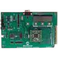
Manufacturer Part Number
MCP3909EV-MCU16
Description
EVALUATION BOARD FOR MCP3909
Manufacturer
Microchip Technology
Datasheets
1.MCP3909T-ISS.pdf
(44 pages)
2.MCP3909T-ISS.pdf
(104 pages)
3.MCP3909EV-MCU16.pdf
(38 pages)
Specifications of MCP3909EV-MCU16
Number Of Adc's
2
Number Of Bits
16
Sampling Rate (per Second)
15k
Data Interface
Serial
Inputs Per Adc
1 Differential
Input Range
±1 V
Voltage Supply Source
Analog and Digital
Operating Temperature
-40°C ~ 85°C
Utilized Ic / Part
MCP3909
Silicon Manufacturer
Microchip
Application Sub Type
ADC
Kit Application Type
Data Converter
Silicon Core Number
MCP3909
Kit Contents
Board
Lead Free Status / RoHS Status
Lead free / RoHS Compliant


MCP3909
3.4
CH0- and CH0+ are the fully differential analog voltage
input channels for the current measurement, containing
a PGA for small-signal input, such as shunt current
sensing. The linear and specified region of this channel
is dependant on the PGA gain. This corresponds to a
maximum differential voltage of ±470 mV/G and
maximum absolute voltage, with respect to A
±1V. Up to ±6V can be applied to these pins without the
risk of permanent damage.
Refer to Section 1.0 “Electrical Characteristics”.
3.5
CH1- and CH1+ are the fully differential analog voltage
input channels for the voltage measurement. The linear
and specified region of these channels have a
maximum differential voltage of ±660 mV and a
maximum absolute voltage of ±1V, with respect to
A
the risk of permanent damage.
Refer to Section 1.0 “Electrical Characteristics”.
3.6
MCLR controls the reset for both delta-sigma ADCs, all
digital registers, the SINC filters for each channel and
all accumulators post multiplier. The MCLR pin is also
used to change pin functionality and enter the serial
interface mode. A logic ‘0’ resets all registers and holds
both ADCs in a Reset condition. The charge stored in
both ADCs is flushed and their output is maintained to
0x0000h. The only block consuming power on the
digital power supply during Reset is the oscillator
circuit.
3.7
REFIN/OUT is the output for the internal 2.4V
reference. This reference has a typical temperature
coefficient of 15 ppm/°C and a tolerance of ±2%. In
addition, an external reference can also be used by
applying voltage to this pin within the specified range.
This pin requires appropriate bypass capacitors to
A
Refer to Section 6.0 “Applications Information”.
3.8
A
circuitry (ADCs, PGA, band gap reference, POR). To
ensure accuracy and noise cancellation, this pin must
be connected to the same ground as D
with a star connection. If an analog ground plane is
available, it is recommended that this device be tied to
this plane of the PCB. This plane should also reference
all other analog circuitry in the system.
DS22025B-page 16
GND
GND
GND
. Up to ±6V can be applied to these pins without
, even when using the internal reference only.
is the ground connection to internal analog
Current Channel (CH0-, CH0+)
Voltage Channel (CH1-,CH1+)
Master Clear (MCLR)
Reference (REFIN/OUT)
Analog Ground (A
GND
)
GND
, preferably
GND
, of
3.9
This dual function pin can act as either the serial clock
input for SPI communication or the F2 selection for the
high-frequency output and low-frequency output pin
ranges, changing the value of the constants F
H
are the frequency constants that define the period of
the output pulses for the device.
3.10
This dual function pin can act as either the serial data
input for SPI communication or the F1 selection for the
high-frequency output and low-frequency output pin
ranges, changing the value of the constants F
H
are the frequency constants that define the period of
the output pulses for the device.
3.11
This dual function pin can act as either the chip select
for SPI communication or the F0 selection for the high-
frequency output and low-frequency output pin ranges
by changing the value of the constants F
used in the device transfer function. F
the frequency constants that define the period of the
output pulses for the device.
3.12
G1 and G0 select the PGA gain (G) on Channel 0 from
four different values: 1, 2, 8 and 16.
3.13
OSC1 and OSC2 provide the master clock for the
device. A resonant crystal or clock source with a similar
sinusoidal waveform must be placed across these pins
to ensure proper operation. The typical clock frequency
specified is 3.579545 MHz. However, the clock
frequency can be within the range of 1 MHz to 4 MHz
without disturbing measurement error. Appropriate
load capacitance should be connected to these pins for
proper operation.
A full-swing, single-ended clock source may be
connected to OSC1 with proper resistors in series to
ensure no ringing of the clock source due to fast
transient edges.
FC
FC
used in the device transfer function. F
used in the device transfer function. F
Serial Clock Input or F2 Frequency
Control Pin
Serial Data Input or F1 Frequency
Control Pin
Chip Select (CS) or F0 Frequency
Control Pin
Gain Control Logic Pins (G1, G0)
Oscillator (OSC1, OSC2)
© 2009 Microchip Technology Inc.
C
and H
C
C
C
and H
and H
and H
FC
C
C
and
and
are
FC
FC
FC
Related parts for MCP3909EV-MCU16
Image
Part Number
Description
Manufacturer
Datasheet
Request
R

Part Number:
Description:
Manufacturer:
Microchip Technology Inc.
Datasheet:
Part Number:
Description:
Manufacturer:
Microchip Technology Inc.
Datasheet:
Part Number:
Description:
Manufacturer:
Microchip Technology Inc.
Datasheet:
Part Number:
Description:
Manufacturer:
Microchip Technology Inc.
Datasheet:
Part Number:
Description:
Manufacturer:
Microchip Technology Inc.
Datasheet:
Part Number:
Description:
Manufacturer:
Microchip Technology Inc.
Datasheet:
Part Number:
Description:
Manufacturer:
Microchip Technology Inc.
Datasheet:
Part Number:
Description:
Manufacturer:
Microchip Technology Inc.
Datasheet: