NCP370GEVB ON Semiconductor, NCP370GEVB Datasheet - Page 10
NCP370GEVB
Manufacturer Part Number
NCP370GEVB
Description
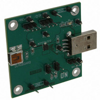
EVAL BOARD FOR NCP370G
Manufacturer
ON Semiconductor
Specifications of NCP370GEVB
Design Resources
NCP370GEVB BOM NCP370GEVB Gerber Files NCP370GEVB Schematic
Main Purpose
Overvoltage Protection
Embedded
No
Utilized Ic / Part
NCP370
Primary Attributes
Overvoltage Protected up to 28V and down to -28V
Secondary Attributes
Reverse Mode
Lead Free Status / RoHS Status
Lead free / RoHS Compliant
For Use With/related Products
NCP370G
Other names
NCP370GEVBOS


ESD Tests
the Input pin. A 1 mF (I.E Murata GRM188R61E105KA12D)
must be placed close to the IN pins. If the IEC61000−4−2 is
not a requirement, a 100 nF/25 V must be placed between IN
and GND.
(Contact) at the input per IEC61000−4−2 (level 4).
electrostatic discharge waveform.
The NCP370 conforms to the IEC61000−4−2, level 4 on
The above configuration supports 15 kV (Air) and 8 kV
Please refer to Figure 8 for the IEC61000−4−2
Figure 8. I
peak
= f(t)/IEC61000−4−2
250
200
150
100
50
0
0
100
Figure 7. Copper heat Spread Area
COPPER HEAT SPREAD AREA (mm
PCB cu thk 2 oz
qJA Curve with
Power Curve with
PCB cu thk 2 oz
200
http://onsemi.com
300
10
PCB cu thk 1 oz
400
qJA Curve with
R
N−MOSFETs to protect the system, connected on OUT pin,
from overvoltage, negative voltage and reverse current
protection. During normal operation, the R
characteristics of the N−MOSFETs give rise to low losses on
V
As example: R
= 800 mA.
V
NMOS Losses = R
Power Curve with
out
out
DS(on)
PCB cu thk 1 oz
The NCP370 includes two internal low R
pin.
= 4.905 V
500
and Dropout
2
)
600
load
= 8 W, Vin= 5 V. R
DS(on)
700
2.5
2
1.5
1
0.5
0
x I
out
2
= 0.155 x 0.8
DS(on)
= 155 mW. I
2
= 0.0992 W
DS(on)
DS(on)
out
Related parts for NCP370GEVB
Image
Part Number
Description
Manufacturer
Datasheet
Request
R

Part Number:
Description:
Positive and Negative Overvoltage Protection
Manufacturer:
ON Semiconductor
Datasheet:
Part Number:
Description:
ON Semiconductor [VOLTAGE REGULATOR]
Manufacturer:
ON Semiconductor
Datasheet:
Part Number:
Description:
357-036-542-201 CARDEDGE 36POS DL .156 BLK LOPRO
Manufacturer:
ON Semiconductor
Datasheet:
Part Number:
Description:
357-036-542-201 CARDEDGE 36POS DL .156 BLK LOPRO
Manufacturer:
ON Semiconductor
Datasheet:
Part Number:
Description:
357-036-542-201 CARDEDGE 36POS DL .156 BLK LOPRO
Manufacturer:
ON Semiconductor
Datasheet:
Part Number:
Description:
357-036-542-201 CARDEDGE 36POS DL .156 BLK LOPRO
Manufacturer:
ON Semiconductor
Datasheet:
Part Number:
Description:
357-036-542-201 CARDEDGE 36POS DL .156 BLK LOPRO
Manufacturer:
ON Semiconductor
Datasheet:
Part Number:
Description:
357-036-542-201 CARDEDGE 36POS DL .156 BLK LOPRO
Manufacturer:
ON Semiconductor
Datasheet:
Part Number:
Description:
357-036-542-201 CARDEDGE 36POS DL .156 BLK LOPRO
Manufacturer:
ON Semiconductor
Datasheet:
Part Number:
Description:
357-036-542-201 CARDEDGE 36POS DL .156 BLK LOPRO
Manufacturer:
ON Semiconductor
Datasheet:
Part Number:
Description:
357-036-542-201 CARDEDGE 36POS DL .156 BLK LOPRO
Manufacturer:
ON Semiconductor
Datasheet:
Part Number:
Description:
357-036-542-201 CARDEDGE 36POS DL .156 BLK LOPRO
Manufacturer:
ON Semiconductor
Datasheet:
Part Number:
Description:
Manufacturer:
ON Semiconductor
Datasheet:
Part Number:
Description:
Manufacturer:
ON Semiconductor
Datasheet: