CDB8421 Cirrus Logic Inc, CDB8421 Datasheet
CDB8421
Specifications of CDB8421


Related parts for CDB8421


CDB8421 Summary of contents
Page 1
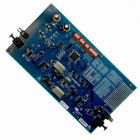
... OLRCK SDOUT Cirrus Logic, Inc. www.cirrus.com Description The CDB8421 demonstration board is an excellent means for evaluating the CS8421 sample rate converter. Evaluation requires a digital signal source, digital analyz- er, and power supplies. System timing can be provided by the CS8421, by the CS8416 phase-locked to its S/PDIF input I/O stake header on-board oscillator ...
Page 2
... CPLD Board Setup ............................................................................................................ 4 1.7 Power ................................................................................................................................. 6 1.8 Grounding and Power Supply Decoupling ......................................................................... 6 2. BLOCK DIAGRAM ................................................................................................................... 8 3. SCHEMATICS .......................................................................................................................... 9 4. LAYOUT ................................................................................................................................. 17 5. APPENDIX A: CS8406 TCBL CONNECTION FOR THE CDB8421 REV. A ......................... 20 6. REFERENCES ........................................................................................................................ 21 7. REVISION HISTORY .............................................................................................................. 22 LIST OF FIGURES Figure 1. Block Diagram.................................................................................................................. 8 Figure 2. Power ............................................................................................................................... 9 Figure 3. CS8416 .......................................................................................................................... 10 Figure 4 ...
Page 3
... The CDB8421 demonstration board is an excellent means for evaluating the CS8421 stereo sample rate converter. Digital audio signal interfaces are provided in the form of S/PDIF receiver and transmitter and PCM clock/data headers. The CDB8421 schematic set is shown in Figures 1 through 9 and the board layout is shown in Figures 10 through 12, and the bill of materials is shown in Table 3. 1.1 ...
Page 4
... Clock and Data Headers The CDB8421 includes headers for input (J8) and output (J11) port clocks and data. These headers can enabled/disabled using S4. When not using these headers, SDIN should be jumpered to SDOUT on both J8 and J11. The pin functions for headers J8 and J11 are shown in Table 7 ...
Page 5
... Left Justified up to 32-bit Data 010 011 100 101 110 Table 4. Switch S3, Serial Input Formats CDB8421 I²S 16-bit Data I²S 20-bit Data I²S 24-bit Data I²S 32-bit Data Left Justified 16-bit Data Left Justified 20-bit Data Left Justified 24-bit Data ...
Page 6
... Header J8 to CS8421 CS8421 to Header J11 Header J11 to CS8406 Input sample rate conversion) Table 5. Switch S4, Board Setup CDB8421 CLOSED Allows Clock I/O and Data Output from CS8416 to Header J8 Allows Clock I/O and Data Input from Header J8 to CS8421 Allows Clock I/O and Data Output from ...
Page 7
... Input/Output I/O for TDM Clocks & Data Table 6. System Connections SIGNAL Master Clock Serial Bit Clock Left-Right (Word) Clock Serial Data (In for J8, Out for J11) Serial Data (Out for J8, In for J11) Ground Table 7. Header Connections (J8 and J11) CDB8421 SIGNAL PRESENT 7 ...
Page 8
... BLOCK DIAGRAM 8 CDB8421 DS641DB3 ...
Page 9
... SCHEMATICS DS641DB3 CDB8421 9 ...
Page 10
... CDB8421 DS641DB3 ...
Page 11
... DS641DB3 CDB8421 11 ...
Page 12
... CDB8421 DS641DB3 ...
Page 13
... DS641DB3 CDB8421 13 ...
Page 14
... CDB8421 DS641DB3 ...
Page 15
... DS641DB3 CDB8421 15 ...
Page 16
... CDB8421 DS641DB3 ...
Page 17
... LAYOUT DS641DB3 CDB8421 17 ...
Page 18
... CDB8421 DS641DB3 ...
Page 19
... DS641DB3 CDB8421 19 ...
Page 20
... APPENDIX A: CS8406 TCBL CONNECTION FOR THE CDB8421 REV. A Pin 15 of U19 on the CDB8421 Rev. A has been lifted. This eliminates the connection to the TCBL pin on the CS8406 part. The pin should remain lifted and no connection to the pin should be reestablished for the board to operate properly. Changes have been made to CDB8421 Rev ...
Page 21
... REFERENCES [1] CS8421 - 32-bit, 192 kHz, Asynchronous, Stereo Sample Rate Converter web page: http://www.cirrus.com/en/products/pro/detail/P1082.html [2] CS8406 - 192 kHz Digital Audio Transmitter web page: http://www.cirrus.com/en/products/pro/detail/P1009.html [3] CS8416 - 192 kHz Digital Audio Receiver web page: http://www.cirrus.com/en/products/pro/detail/P1005.html DS641DB3 CDB8421 21 ...
Page 22
... C irrus Logic, C irrus, and the Cirrus Logic logo designs are tradem arks of C irrus Logic, Inc other brand and product nam es in this docum ent tradem arks or service m arks of their respective owners. 22 Changes 1st Release Corrected figure caption on page 10. 2nd Release -Updated “Schematics” on page 9 and “Layout” on page 17. -Updated “References” on page 21. Table 8. Revision History .cirrus.com CDB8421 DS641DB3 ...