AD9551/PCBZ Analog Devices Inc, AD9551/PCBZ Datasheet - Page 9
AD9551/PCBZ
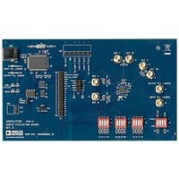
Manufacturer Part Number
AD9551/PCBZ
Description
BOARD EVAL FOR AD9951
Manufacturer
Analog Devices Inc
Datasheet
1.AD9551PCBZ.pdf
(40 pages)
Specifications of AD9551/PCBZ
Main Purpose
Timing, Clock Generator
Embedded
No
Utilized Ic / Part
AD9551
Primary Attributes
2 Inputs, 2 Outputs, VCO
Secondary Attributes
Graphical User Interface, USB Interface
Silicon Manufacturer
Analog Devices
Application Sub Type
Clock Generator
Kit Application Type
Clock & Timing
Silicon Core Number
AD9551
Kit Contents
Board
Lead Free Status / RoHS Status
Lead free / RoHS Compliant


PIN CONFIGURATION AND FUNCTION DESCRIPTIONS
Table 12. Pin Function Descriptions
Pin
No.
9, 23,
27, 34
30, 31
4
3
5
6
13
14
15
7
11
12
33
32
29
28
17
26
25
16
8
10
22
24
35
36
37
38
Mnemonic
VDD
GND
REFA
REFA
REFB
REFB
CS
SCLK
SDIO
RESET
XTL0
XTL1
OUT1
OUT1
OUT2
OUT2
LF
OUTPUT PLL LOCKED
INPUT PLL LOCKED
OUTSEL
LDO_IPDIG
LDO_XTAL
LDO_VCO
LDO_1.8
A0
A1
A2
A3
Type
P
P
I
I
I
I
I
I
I/O
I
I
I
O
O
O
O
I/O
O
O
I
P/O
P/O
P/O
P/O
I
I
I
I
1
Description
Power Supply Connection (3.3 V Analog Supply).
Analog Ground.
Analog Input (Active High)—Reference Clock Input A.
Analog Input (Active High)—Complementary Reference Clock Input A.
Analog Input (Active High)—Reference Clock Input B.
Analog Input (Active High)—Complementary Reference Clock Input B.
Digital Input Chip Select (Active Low).
Serial Data Clock.
Digital Serial Data Input/Output.
Digital Input (Active High). Resets internal logic to default states. This pin has an internal 100 kΩ
pull-up resistor, so the default state of the device is reset.
Pin for Connecting an External Crystal (20 MHz to 30 MHz).
Pin for Connecting an External Crystal (20 MHz to 30 MHz).
Loop Filter Node for the Output PLL. Connect an external 12 nF capacitor (100 nF in 19.44 MHz
mode) from this pin to Pin 22 ( LDO_VCO).
Active High Locked Status Indicator for the Output PLL.
Active High Locked Status Indicator for the Input PLL.
Logic 0 selects LVDS, and Logic 1 selects LVPECL-compatible levels for both OUT1 and OUT2
when the outputs are not under SPI port control. Can be overridden via the programming registers.
LDO Decoupling Pin. Connect a 0.47 μF decoupling capacitor from this pin to ground.
LDO Decoupling Pin. Connect a 0.47 μF decoupling capacitor from this pin to ground.
LDO Decoupling Pin. Connect a 0.47 μF decoupling capacitor from this pin to ground.
LDO Decoupling Pin. Connect a 0.47 μF decoupling capacitor from this pin to ground.
Control Pin. Selects preset values for the REFA dividers.
Control Pin. Selects preset values for the REFA dividers.
Control Pin. Selects preset values for the REFA dividers.
Control Pin. Selects preset values for the REFA dividers.
Square Wave Clocking Output 1.
Complementary Square Wave Clocking Output 1.
Square Wave Clocking Output 2.
Complementary Square Wave Clocking Output 2.
LDO_IPDIG
LDO_XTAL
NOTES
1. EXPOSED DIE PAD MUST BE CONNECTED TO GND.
RESET
REFB
REFB
REFA
REFA
VDD
B2
B3
10
1
2
3
4
5
6
7
8
9
Figure 3. Pin Configuration
Rev. B | Page 9 of 40
PIN 1
INDICATOR
(Not to Scale)
AD9551
TOP VIEW
30 GND
29 OUT2
28 OUT2
27 VDD
26 OUTPUT PLL LOCKED
25 INPUT PLL LOCKED
24 LDO_1.8
23 VDD
22 LDO_VCO
21 Y0
AD9551
Related parts for AD9551/PCBZ
Image
Part Number
Description
Manufacturer
Datasheet
Request
R


Part Number:
Description:
±1.7g Dual-Axis IMEMS Accelerometer Evaluation Board
Manufacturer:
Analog Devices Inc
Datasheet:

Part Number:
Description:
Inertial Sensor Evaluation System
Manufacturer:
Analog Devices Inc
Datasheet:
Part Number:
Description:
Manufacturer:
Analog Devices Inc
Datasheet:
Part Number:
Description:
Manufacturer:
Analog Devices Inc
Datasheet:
Part Number:
Description:
Manufacturer:
Analog Devices Inc
Datasheet:
Part Number:
Description:
Manufacturer:
Analog Devices Inc
Datasheet:
Part Number:
Description:
Manufacturer:
Analog Devices Inc
Datasheet:
Part Number:
Description:
Manufacturer:
Analog Devices Inc
Datasheet:
Part Number:
Description:
Manufacturer:
Analog Devices Inc
Datasheet:
Part Number:
Description:
Manufacturer:
Analog Devices Inc
Datasheet:
Part Number:
Description:
Manufacturer:
Analog Devices Inc
Datasheet:
Part Number:
Description:
Manufacturer:
Analog Devices Inc
Datasheet: