AD9551/PCBZ Analog Devices Inc, AD9551/PCBZ Datasheet - Page 27
AD9551/PCBZ
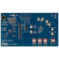
Manufacturer Part Number
AD9551/PCBZ
Description
BOARD EVAL FOR AD9951
Manufacturer
Analog Devices Inc
Datasheet
1.AD9551PCBZ.pdf
(40 pages)
Specifications of AD9551/PCBZ
Main Purpose
Timing, Clock Generator
Embedded
No
Utilized Ic / Part
AD9551
Primary Attributes
2 Inputs, 2 Outputs, VCO
Secondary Attributes
Graphical User Interface, USB Interface
Silicon Manufacturer
Analog Devices
Application Sub Type
Clock Generator
Kit Application Type
Clock & Timing
Silicon Core Number
AD9551
Kit Contents
Board
Lead Free Status / RoHS Status
Lead free / RoHS Compliant


By default, a read request reads the register value that is currently
in use by the AD9551. However, setting Register 0x04[0] = 1
causes the buffered registers to be read instead. The buffered
registers are the ones that take effect during the next I/O update.
The AD9551 uses Register 0x00 to Register 0x34. Although the
AD9551 serial control port allows both 8-bit and 16-bit instruc-
tions, the 8-bit instruction mode provides access to five address
bits (Address Bits[A4:A0]) only, which restricts its use to Address
Space 0x00 to Address Space 0x01. The AD9551 defaults to 16-bit
instruction mode on power-up, and the 8-bit instruction mode is
not supported.
INSTRUCTION WORD (16 BITS)
The MSB of the instruction word (see Table 20) is R/
indicates whether the instruction is a read or a write. The next
two bits, W1 and W0, are the transfer length in bytes. The final
13 bits are the address bits (Address Bits[A12:A0]) at which the
read or write operation is to begin.
For a write, the instruction word is followed by the number of
bytes of data indicated Bits[W1:W0], which is interpreted
according to Table 19.
Address Bits[A12:A0] select the address within the register map
that is written to or read from during the data transfer portion
of the communication cycle. The AD9551 uses all of the 13-bit
address space. For multibyte transfers, this address is the starting
byte address.
Table 20. Serial Control Port, 16-Bit Instruction Word, MSB First
MSB
I15
R/W
Table 21. Definition of Terms Used in Serial Control Port Timing Diagrams
Parameter
t
t
t
t
t
t
t
t
Figure 25. Relationship Between the Serial Control Port Register Buffers and
CLK
DV
DS
DH
S
H
HIGH
LOW
SCLK
SDIO
CS
I14
W1
14
15
13
CONTROL
SERIAL
PORT
I13
W0
Description
Period of SCLK
Read data valid time (time from falling edge of SCLK to valid data on SDIO)
Setup time between data and rising edge of SCLK
Hold time between data and rising edge of SCLK
Setup time between CS and SCLK
Hold time between CS and SCLK
Minimum period that SCLK should be in a logic high state
Minimum period that SCLK should be in a logic low state
the Control Registers
I12
A12
INPUT/OUTPUT
REGISTER
EXECUTE AN
UPDATE
UPDATE
I11
A11
AD9551
I10
A10
CORE
W
, which
I9
A9
Rev. B | Page 27 of 40
I8
A8
MSB/LSB FIRST TRANSFERS
The AD9551 instruction word and byte data can be MSB first or
LSB first. The default for the AD9551 is MSB first. The LSB first
mode can be set by writing a 1 to Register 0x00[6] and requires
that an I/O update be executed. Immediately after the LSB first
bit is set, all serial control port operations are changed to LSB
first order.
When MSB first mode is active, the instruction and data bytes
must be written from MSB to LSB. Multibyte data transfers in
MSB first format start with an instruction byte that includes the
register address of the most significant data byte. Subsequent
data bytes must follow in order from high address to low address.
In MSB first mode, the serial control port internal address gen-
erator decrements for each data byte of the multibyte transfer cycle.
When LSB first = 1 (LSB first), the instruction and data bytes must
be written from LSB to MSB. Multibyte data transfers in LSB first
format start with an instruction byte that includes the register
address of the least significant data byte followed by multiple data
bytes. The serial control port internal byte address generator
increments for each data byte of the multibyte transfer cycle.
The AD9551 serial control port register address decrements from
the register address just written toward 0x00 for multibyte I/O
operations if the MSB first mode is active (default). If the LSB
first mode is active, the serial control port register address
increments from the address just written toward 0x34 for
multibyte I/O operations.
Unused addresses are not skipped during multibyte I/O operations.
The user should write the default value to a reserved register and
should write only zeros to unmapped registers. Note that it is more
efficient to issue a new write command than to write the default
value to more than two consecutive reserved (or unmapped)
registers.
I7
A7
I6
A6
I5
A5
I4
A4
I3
A3
I2
A2
I1
A1
AD9551
LSB
I0
A0
Related parts for AD9551/PCBZ
Image
Part Number
Description
Manufacturer
Datasheet
Request
R


Part Number:
Description:
±1.7g Dual-Axis IMEMS Accelerometer Evaluation Board
Manufacturer:
Analog Devices Inc
Datasheet:

Part Number:
Description:
Inertial Sensor Evaluation System
Manufacturer:
Analog Devices Inc
Datasheet:
Part Number:
Description:
Manufacturer:
Analog Devices Inc
Datasheet:
Part Number:
Description:
Manufacturer:
Analog Devices Inc
Datasheet:
Part Number:
Description:
Manufacturer:
Analog Devices Inc
Datasheet:
Part Number:
Description:
Manufacturer:
Analog Devices Inc
Datasheet:
Part Number:
Description:
Manufacturer:
Analog Devices Inc
Datasheet:
Part Number:
Description:
Manufacturer:
Analog Devices Inc
Datasheet:
Part Number:
Description:
Manufacturer:
Analog Devices Inc
Datasheet:
Part Number:
Description:
Manufacturer:
Analog Devices Inc
Datasheet:
Part Number:
Description:
Manufacturer:
Analog Devices Inc
Datasheet:
Part Number:
Description:
Manufacturer:
Analog Devices Inc
Datasheet: