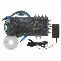
AD9520-1/PCBZ Analog Devices Inc, AD9520-1/PCBZ Datasheet - Page 19

AD9520-1/PCBZ
Manufacturer Part Number
AD9520-1/PCBZ
Description
BOARD EVAL FOR AD9520-1
Manufacturer
Analog Devices Inc
Specifications of AD9520-1/PCBZ
Design Resources
Synchronizing Multiple AD9910 1 GSPS Direct Digital Synthesizers (CN0121) Phase Coherent FSK Modulator (CN0186)
Main Purpose
Timing, Clock Generator
Embedded
No
Utilized Ic / Part
AD9520-1
Primary Attributes
12 LVPECL/24 CMOS Output Clock Generator with 2.5 GHz VCO
Secondary Attributes
SPI and I2C Compatible Control Port
Silicon Manufacturer
Analog Devices
Application Sub Type
PLL Clock Synthesizer
Kit Application Type
Clock & Timing
Silicon Core Number
AD9520-0, AD9520-2, AD9520-2
Silicon Family Name
AD9520-X
Rohs Compliant
Yes
Lead Free Status / RoHS Status
Lead free / RoHS Compliant
Pin No.
15
16
17
18
19, 59
20
21
22
23
24
25
26
27, 35,
46, 54
28
29
30
31
33
34
36
37
38
39
42
43
44
45
47
Input/
Output
I
I
I/O
O
I
I
I
I
I
I
O
O
I
O
O
O
O
O
O
O
O
O
O
O
O
O
O
O
Pin
Type
3.3 V CMOS
3.3 V CMOS
3.3 V CMOS
3.3 V CMOS
GND
Three-level
logic
Three-level
logic
3.3 V CMOS
3.3 V CMOS
3.3 V CMOS
LVPECL or
CMOS
LVPECL or
CMOS
Power
LVPECL or
CMOS
LVPECL or
CMOS
LVPECL or
CMOS
LVPECL or
CMOS
LVPECL or
CMOS
LVPECL or
CMOS
LVPECL or
CMOS
LVPECL or
CMOS
LVPECL or
CMOS
LVPECL or
CMOS
LVPECL or
CMOS
LVPECL or
CMOS
LVPECL or
CMOS
LVPECL or
CMOS
LVPECL or
CMOS
Mnemonic
CS
SCLK/SCL
SDIO/SDA
SDO
GND
SP1
SP0
EEPROM
RESET
PD
OUT9 (OUT9A)
OUT9 (OUT9B)
VS_DRV
OUT10 (OUT10A)
OUT10 (OUT10B)
OUT11 (OUT11A)
OUT11 (OUT11B)
OUT6 (OUT6A)
OUT6 (OUT6B)
OUT7 (OUT7A)
OUT7 (OUT7B)
OUT8 (OUT8A)
OUT8 (OUT8B)
OUT5 (OUT5B)
OUT5 (OUT5A)
OUT4 (OUT4B)
OUT4 (OUT4A)
OUT3 (OUT3B)
Description
Serial Control Port Chip Select; Active Low. This pin has an internal 30 kΩ
pull-up resistor.
Serial Control Port Clock Signal. This pin has an internal 30 kΩ pull-down resistor
in SPI mode but is high impedance in I²C mode.
Serial Control Port Bidirectional Serial Data In/Out.
Serial Control Port Unidirectional Serial Data Out.
Ground Pins.
Select SPI or I²C as the serial interface port and select the I²C slave address in I²C
mode. Three-level logic. This pin is internally biased for the open logic level.
Select SPI or I²C as the serial interface port and select the I²C slave address in I²C
mode. Three-level logic. This pin is internally biased for the open logic level.
Setting this pin high selects the register values stored in the internal EEPROM to
be loaded at reset and/or power-up. Setting this pin low causes the AD9520 to
load the hard-coded default register values at power-up/reset. This pin has an
internal 30 kΩ pull-down resistor.
Chip Reset, Active Low. This pin has an internal 30 kΩ pull-up resistor.
Chip Power-Down, Active Low. This pin has an internal 30 kΩ pull-up resistor.
Clock Output. This pin can be configured as one side of a differential LVPECL
output or as a single-ended CMOS output.
Clock Output. This pin can be configured as one side of a differential LVPECL
output or as a single-ended CMOS output.
Output Driver Power Supply Pins. As a group, these pins can be set to either
2.5 V or 3.3 V. All four pins must be set to the same voltage.
Clock Output. This pin can be configured as one side of a differential LVPECL
output or as a single-ended CMOS output.
Clock Output. This pin can be configured as one side of a differential LVPECL
output or as a single-ended CMOS output.
Clock Output. This pin can be configured as one side of a differential LVPECL
output or as a single-ended CMOS output.
Clock Output. This pin can be configured as one side of a differential LVPECL
output or as a single-ended CMOS output.
Clock Output. This pin can be configured as one side of a differential LVPECL
output or as a single-ended CMOS output.
Clock Output. This pin can be configured as one side of a differential LVPECL
output or as a single-ended CMOS output.
Clock Output. This pin can be configured as one side of a differential LVPECL
output, or as a single-ended CMOS output.
Clock Output. This pin can be configured as one side of a differential LVPECL
output or as a single-ended CMOS output.
Clock Output. This pin can be configured as one side of a differential LVPECL
output or as a single-ended CMOS output.
Clock Output. This pin can be configured as one side of a differential LVPECL
output or as a single-ended CMOS output.
Clock Output. This pin can be configured as one side of a differential LVPECL
output or as a single-ended CMOS output.
Clock Output. This pin can be configured as one side of a differential LVPECL
output or as a single-ended CMOS output.
Clock Output. This pin can be configured as one side of a differential LVPECL
output or as a single-ended CMOS output.
Clock Output. This pin can be configured as one side of a differential LVPECL
output or as a single-ended CMOS output.
Clock Output. This pin can be configured as one side of a differential LVPECL
output or as a single-ended CMOS output.
Rev. 0 | Page 19 of 84
AD9520-1


