ADNK-3083 Avago Technologies US Inc., ADNK-3083 Datasheet - Page 3
ADNK-3083
Manufacturer Part Number
ADNK-3083
Description
KIT REFERENCE DESIGN ADNS-3080
Manufacturer
Avago Technologies US Inc.
Specifications of ADNK-3083
Main Purpose
Reference Design, Optical Mouse
Utilized Ic / Part
ADNS-3080, CY7C63743-PXC, CY7C63743A
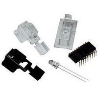
Kit Contents
ADNS-3080 Sensor, UP, Hardware And Documentation
Peak Reflow Compatible (260 C)
Yes
Tool / Board Applications
Optical Mouse Sensors
Description/function
Optical Mouse Sensor Kit
Interface Type
USB
Product
Display Modules
Touch Panel
No Touch Panel
Development Tool Type
Hardware / Software - Dev Kit (Dev Tool)
Rohs Compliant
Yes
For Use With
ADNS-3080
Lead Free Status / RoHS Status
Lead free / RoHS Compliant
Secondary Attributes
-
Embedded
-
Primary Attributes
-
Lead Free Status / Rohs Status
Details
For Use With/related Products
CY7C63743-PXC, CY7C63743A-PC
Lead Free Status / RoHS Status
Lead free / RoHS Compliant, Lead free / RoHS Compliant


Serial Peripheral Interface (SPI)
The CY7C63743-PXC provides a SPI compatible interface.
The SPI circuit supports byte serial transfer in either
Master or Slave mode. The integrated SPI circuit allows
the CY7C63743-PXC to communicate with an external
SPI compatible hardware, in this case the ADNS-3080
sensor.
Hardware Implementation
The standard hardware to implement a mouse is shown
in Figure 2. For X and Y movement, the optical mouse
sensor is used. The Z wheel movement is detected by
another set of optical encoder that outputs quadrature
signals. For each button there is a switch that is pulled up
internally by the built-in in pull up resistors. The D-line is
pulled up via a 1.3k ohm resistor connected to the VREG
pin.
Firmware Configurable GPIO
The reference firmware is configured to use the GPIO pins
as shown in the schematic under Appendix A. However, it
may be more optimal to use a different I/O configuration
to meet the mechanical constraints of PCB design. The
reference firmware is designed to be easily configured
to another set of pin connections. This is accomplished
through changes in the I/O definitions at the beginning
Figure 2. CY7C63743-PXC –ADNS-3080 Optical Mouse Hardware Block Diagram.
optical mouse sensor
Avago ADNS-3080
Wheel Button
Right Button
Left Button
Z Optics
Z LED
MISO
MOSI
NCS
SCLK
CY7C63743A-PC
USB Controller
Cypress
enCoRe
of the adns- 3080.asm listing. The following statements
are the pin definitions as they exist today. The firmware
will use these definitions to read and configure the GPIO
pins, without any other modifications.
Communications between the CY7C63743-PXC and the
ADNS-3080 are done through the integrated SPI inter-
face. The serial port cannot be activated while the chip
is in power down mode (NPD low) or reset (RESET high).
When the SPI is enabled thru P0.4 (NCS), P0.7 (SCLK),
P0.6 (MISO), and P0.5 (MOSI) GPIO pins serve as special
functions enabling the SPI interface to talk with the ex-
ternal hardware. (Sensor) During normal operation, the
CY7C63743-PXC SPI is always configured as a Master to
output the serial clock on P0.7. So, the USB microcon-
troller always initiates communication. Data sent by the
ADNS-3080 optical sensor is received on the P0.6 (MISO),
and data is shifted out to the same sensor through P0.5
(MOSI). See schematic in Appendix A. When writing to
the ADNS-3080, the microcontroller drives both SCLK
and MOSI lines. When reading from the ADNS-3080, the
microcontroller drives both SCLK and MOSI lines initially.
After tSRAD delay, the ADNS-3080 will drive the data via
MISO. The microcontroller is only driving the SCLK line (
for the serial interface).
VREG
SCLK/SDATA
D+/D-
1.3 k Ohm
USB/PS2 Interface
Related parts for ADNK-3083
Image
Part Number
Description
Manufacturer
Datasheet
Request
R

Part Number:
Description:
ADNK-3000 Sample Kit
Manufacturer:
Avago Technologies US Inc.
Datasheet:

Part Number:
Description:
KIT REFERENCE DESIGN ADNK-3060
Manufacturer:
Avago Technologies US Inc.
Datasheet:

Part Number:
Description:
KIT REFERENCE DESIGN ADNK-5030
Manufacturer:
Avago Technologies US Inc.
Datasheet:
Part Number:
Description:
KIT DES BLUETOOTH OPT ADNK-3043
Manufacturer:
Avago Technologies US Inc.
Datasheet:
Part Number:
Description:
KIT SAMPLE FOR ADNS-5030
Manufacturer:
Avago Technologies US Inc.
Datasheet:
Part Number:
Description:
KIT SAMPLE OPT MOUSE ADNS-3550
Manufacturer:
Avago Technologies US Inc.
Datasheet:
Part Number:
Description:
KIT SAMPLE OPT MOUSE ADNS-5000
Manufacturer:
Avago Technologies US Inc.
Datasheet:

Part Number:
Description:
KIT SAMPLE OPTICAL MOUSE A5050
Manufacturer:
Avago Technologies US Inc.
Datasheet:
Part Number:
Description:
KIT SAMPLE OPT MOUSE ADNS-5060
Manufacturer:
Avago Technologies US Inc.
Datasheet:

Part Number:
Description:
OPTOCOUPLER GATE DRV 2A 16-SOIC
Manufacturer:
Avago Technologies US Inc.
Datasheet:
Part Number:
Description:
OPTOCOUPLER 2CH 2.5A 16-SOIC
Manufacturer:
Avago Technologies US Inc.
Datasheet:

Part Number:
Description:
OPTOCOUPLER GATE DRV 0.4A 16SOIC
Manufacturer:
Avago Technologies US Inc.
Datasheet:

Part Number:
Description:
OPTOCOUPLER 2.0A 250KHZ 8-DIP
Manufacturer:
Avago Technologies US Inc.
Datasheet:

Part Number:
Description:
OPTOCOUPLER 2.0A 250KHZ GW 8-SMD
Manufacturer:
Avago Technologies US Inc.
Datasheet: