EVAL-AD7877EBZ Analog Devices Inc, EVAL-AD7877EBZ Datasheet - Page 19
EVAL-AD7877EBZ
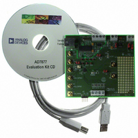
Manufacturer Part Number
EVAL-AD7877EBZ
Description
BOARD EVALUATION FOR AD7877
Manufacturer
Analog Devices Inc
Datasheets
1.AD7877ACBZ-REEL7.pdf
(44 pages)
2.EVAL-AD7877EBZ.pdf
(16 pages)
3.EVAL-AD7877EBZ.pdf
(44 pages)
Specifications of EVAL-AD7877EBZ
Main Purpose
Interface, Touch Screen Controller
Embedded
No
Utilized Ic / Part
AD7877
Primary Attributes
4-Wire Resistive Touch Screen Controller, SPI Interface, On-Chip: Temp Sensor, Voltage Reference, 8-Bit DAC
Secondary Attributes
USB GUI, LCD Noise Reduction Feature, 2.7 ~ 5.25 V, Wake Up on Touch Feature
Lead Free Status / RoHS Status
Lead free / RoHS Compliant


AUXILIARY INPUTS
The AD7877 has three auxiliary analog inputs, AUX1 to AUX3.
These channels have a full-scale input range from 0 V to V
The ADC channel addresses for AUX1 to AUX3 are 0011b,
0100b, and 0101b, and the results are stored in Register 10011b,
Register 10100b, and Register 10101b. These pins can also be
reconfigured as general-purpose logic inputs/outputs, as
described in the GPIO Configuration section.
LIMIT COMPARISON
The AUX1 measurement, the two battery measurements, and
the TEMP1 measurement can all be compared with high and
low limits, and an out-of-limit result that generates an alarm
output at the ALERT pin. The limits are stored in registers with
addresses from 00100b to 01011b. After a measurement from
any one of the four channels is converted, it is compared with
the corresponding high and low limits. An out-of-limit result
sets one of the status bits in the alert status/enable register. For
details on these and other registers, see the Register Maps and
Detailed Register Descriptions sections. For details on writing
and reading data, see the Serial Interface section.
As described in the Single Conversion Method section, the
temperature comparison is made using the result of the TEMP1
measurement, that is, the diode forward voltage. Because the
temperature coefficient of the diode is known but the actual
forward voltage can have a wide tolerance, it is not possible
to program the high and low limit registers with predeter-
mined values.
REF
Rev. B | Page 19 of 44
.
Instead, it is necessary to calibrate the temperature measure-
ment, calculate the TEMP1 readings at the high and low limit
temperatures, and then program those values into the limit
registers, as follows:
1.
2.
3.
4.
5.
Example:
The internal 2.5 V reference is used.
1.
2.
3.
4.
5.
Calculate
LSB per degree = −2.1 mV/(V
Save the calibration reading D
Temperature T
Subtract T
get the difference in degrees between the limit
temperatures and the calibration temperature.
Multiply this value by LSB per degree to obtain the
value in LSBs.
Add these values to the digital value at the calibration
temperature to get the digital high and low limit values.
T
LSB per degree = −2.1 × 10
D
D
D
HIGH
CAL
HIGH
LOW
= 983 decimal at 25°C.
= (−10 − 25) × −3.44 + 983 = 1103.
= +65°C and T
= (65 − 25) × −3.44 + 983 = 845.
CAL
from limit temperatures T
CAL
.
LOW
= −10°C.
−3
/(2.5/4096) = −3.44.
REF
CAL
/4096).
at Calibration
HIGH
and T
AD7877
LOW
to
Related parts for EVAL-AD7877EBZ
Image
Part Number
Description
Manufacturer
Datasheet
Request
R


Part Number:
Description:
BOARD EVAL FOR SI270X-A
Manufacturer:
Silicon Laboratories Inc
Datasheet:

Part Number:
Description:
BUCK CONV REF DESIGN KIT IP1201
Manufacturer:
International Rectifier
Datasheet:
Part Number:
Description:
BOARD DEMO SYNC DUAL BUCK CNVTER
Manufacturer:
International Rectifier
Datasheet:
Part Number:
Description:
BOARD DEMO SYNC BUCK CONVETER
Manufacturer:
International Rectifier
Datasheet:

Part Number:
Description:
EVALBOARD/EB Omnidirectional microphone - Analog
Manufacturer:
Analog Devices
Datasheet:
Part Number:
Description:
EVALBOARD/EB Omnidirectional microphone - Analog
Manufacturer:
Analog Devices
Datasheet:


Part Number:
Description:
BOARD EVAL LED DRIVER LT3756
Manufacturer:
Linear Technology
Datasheet:

Part Number:
Description:
BOARD EVAL FOR AD7741/7742
Manufacturer:
Analog Devices Inc
Datasheet:

Part Number:
Description:
±1.7g Dual-Axis IMEMS Accelerometer Evaluation Board
Manufacturer:
Analog Devices Inc
Datasheet:

Part Number:
Description:
IC MULTIPLIER ANALOG 8-SOIC T/R
Manufacturer:
Analog Devices Inc
Datasheet:

Part Number:
Description:
IC ANALOG MULTIPLIER 8-DIP
Manufacturer:
Analog Devices Inc
Datasheet:
Part Number:
Description:
IC ANALOG MULTIPLIER 8-SOIC
Manufacturer:
Analog Devices Inc
Datasheet:
Part Number:
Description:
IC ANALOG MULTIPLIER 8-DIP
Manufacturer:
Analog Devices Inc
Datasheet: