MCP3421DM-BFG Microchip Technology, MCP3421DM-BFG Datasheet - Page 8
MCP3421DM-BFG
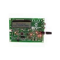
Manufacturer Part Number
MCP3421DM-BFG
Description
BOARD DEMO FOR MCP3421
Manufacturer
Microchip Technology
Datasheets
1.MCP3421A2T-ECH.pdf
(42 pages)
2.MCP3421DM-BFG.pdf
(26 pages)
3.MCP3421A0T-ECH.pdf
(30 pages)
Specifications of MCP3421DM-BFG
Main Purpose
Power Management, Battery Gauge
Utilized Ic / Part
MCP3421
Processor To Be Evaluated
MCP3421
Lead Free Status / RoHS Status
Lead free / RoHS Compliant
Secondary Attributes
-
Embedded
-
Primary Attributes
-
Lead Free Status / RoHS Status
Lead free / RoHS Compliant, Lead free / RoHS Compliant


MCP3421
The output codes will not roll-over if the input voltage
exceeds the maximum input range. In this case, the
code will be locked at 0111...11 for all voltages
greater than +(V
voltages less than -V
of output codes of various input levels using 18 bit
conversion mode.
minimum and maximum codes for each data rate
option.
The output code is given by:
EQUATION 4-1:
The LSB of the code is given by:
EQUATION 4-2:
TABLE 4-1:
TABLE 4-2:
DS22003D-page 8
Where:
Bit Resolutions
Output Code
Input Voltage (V)
N = number of bits
V
REF
12 bits
14 bits
16 bits
18 bits
< -V
-1 LSB
-2 LSB
≥
- V
2 LSB
1 LSB
V
- 1 LSB
0
REF
REF
REF
=
REF
LSB
LSB SIZE OF VARIOUS BIT
CONVERSION MODES
EXAMPLE OF OUTPUT CODE
FOR 18 BITS
(
Table 4-3
Max Code
REF
- 1 LSB) and 1000...00 for
=
.
1 mV
250 µV
62.5 µV
15.625 µV
Table 4-2
2 2.048V
--------------------------
×
011111111111111111
011111111111111111
000000000000000010
000000000000000001
000000000000000000
111111111111111111
111111111111111110
100000000000000000
100000000000000000
2
+
shows an example of
N
1
)
×
Digital Code
LSB (V)
shows an example
-------------------------------------- -
(
V
IN
2.048V
+
–
V
IN
-
)
TABLE 4-3:
4.6
The device performs a self-calibration of offset and
gain for each conversion. This provides reliable
conversion results from conversion-to-conversion over
variations in temperature as well as power supply
fluctuations.
4.7
The MCP3421 uses a switched-capacitor input stage
using a 3.2 pF sampling capacitor. This capacitor is
switched (charged and discharged) at a rate of the
sampling frequency that is generated by the on-board
clock. The differential mode impedance varies with the
PGA settings. The typical differential input impedance
during a normal mode operation is given by:
Since the sampling capacitor is only switching to the
input pins during a conversion process, the above input
impedance is only valid during conversion periods. In a
low power standby mode, the above impedance is not
presented at the input pins. Therefore, only a leakage
current due to ESD diode is presented at the input pins.
The conversion accuracy can be affected by the input
signal source impedance when any external circuit is
connected to the input pins. The source impedance
adds to the internal impedance and directly affects the
time required to charge the internal sampling capacitor.
Therefore, a large input source impedance connected
to the input pins can increase the system performance
errors such as offset, gain, and integral nonlinearity
(INL) errors. Ideally, the input source impedance
should be zero. This can be achievable by using an
operational amplifier with a closed-loop output
impedance of tens of ohms.
Number
Note:
of Bits
12
14
16
18
Self-Calibration
Input Impedance
Maximum n-bit code = 2
Minimum n-bit code = -1 x 2
Data Rate
3.75 SPS
240 SPS
60 SPS
15 SPS
Z
IN
MINIMUM AND MAXIMUM
CODES
(f) = 2.25 M
© 2007 Microchip Technology Inc.
Minimum
-131072
-32768
-2048
-8192
Code
Ω
/PGA
n-1
- 1
n-1
Maximum
131071
32767
Code
2047
8191
Related parts for MCP3421DM-BFG
Image
Part Number
Description
Manufacturer
Datasheet
Request
R

Part Number:
Description:
18-Bit Analog-to-Digital Converter with I2C Interface and On-Board Reference
Manufacturer:
Microchip Technology
Datasheet:

Part Number:
Description:
Manufacturer:
Microchip Technology Inc.
Datasheet:
Part Number:
Description:
Manufacturer:
Microchip Technology Inc.
Datasheet:
Part Number:
Description:
Manufacturer:
Microchip Technology Inc.
Datasheet:
Part Number:
Description:
Manufacturer:
Microchip Technology Inc.
Datasheet:
Part Number:
Description:
Manufacturer:
Microchip Technology Inc.
Datasheet:
Part Number:
Description:
Manufacturer:
Microchip Technology Inc.
Datasheet:
Part Number:
Description:
Manufacturer:
Microchip Technology Inc.
Datasheet:
Part Number:
Description:
Manufacturer:
Microchip Technology Inc.
Datasheet: