MXSIGDM Microchip Technology, MXSIGDM Datasheet - Page 19
MXSIGDM
Manufacturer Part Number
MXSIGDM
Description
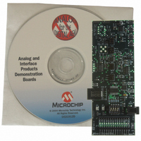
BOARD DEMO PICTAIL MIXED SIGNAL
Manufacturer
Microchip Technology
Series
PICtail™r
Datasheet
1.MXSIGDM.pdf
(54 pages)
Specifications of MXSIGDM
Main Purpose
Mixed Signal for MCU: ADC, DAC,
Embedded
Yes, MCU, 8-Bit
Utilized Ic / Part
TX132x,MCP330x,320x,494x,3221,3201,1525,1541
Primary Attributes
3 ADCs, 3 DACs, 2 Voltage References, 5V LDO
Secondary Attributes
DIP Switches, 2 LEDs, PIC16F767
Processor To Be Evaluated
TC132x, MCP330x, MCP320x, MCP492x, MCP3221, MCP3021, MCP15x
Interface Type
I2C, SPI
Lead Free Status / RoHS Status
Contains lead / RoHS non-compliant
Lead Free Status / RoHS Status
Lead free / RoHS Compliant, Contains lead / RoHS non-compliant


2.4
2004 Microchip Technology Inc.
RUNNING THE DEMOS
The Mixed Signal PICtail™ Demo Board was designed to utilize the PIC16F767
located on the PCB or a PICmicro microcontroller operating on the PICkit™ 1 Flash
Starter Kit board. This Mixed Signal PICtail™ Demo Board User’s Guide will only
discuss the stand-alone operation utilizing the PIC16F767.
2.4.1
The Mixed Signal PICtail™ Demo Board can be powered by either the PICkit™ 1 Flash
Starter Kit’s V
maximum). The onboard TC55 5.0V LDO produces a regulated 5.0V supply to operate
the analog devices under test. The Mixed Signal PICtail™ Demo Board User’s Guide
assumes the standard 9V power supply that comes with many of Microchip’s develop-
ment tools (including the MPLAB
provided for your convenience.
With the default firmware programmed into the PIC16F767, the LED’s should
alternately flash for approximately two seconds upon power-up.
2.4.2
S
have one terminal tied to V
with the PIC16F767 PORTB<4:7> I/O port. These pins have an internal weak pull-up
to prevent the I/O from floating when the corresponding DIP switch is open. The DIP
switch is labeled with an arrow indicating the “on” (or closed) position of the switch.
When the DIP switch is on, the I/O pin is pulled down to V
interpret this as a “0”. The binary combination of these four DIP switches determine the
mode of operation.
Refer to Section 2.3.2 “The Embedded System Firmware” for operational details for
each mode.
2.4.3
Jumper JP1 is located in the center of the board closest to the PICmicro microcontroller
and its MPLAB ICD 2 connector. JP1 consists of three pairs of jumper pins. The
lower-two pins are connected to A
The top-two pins are connected to A
Refer to Figure 2-2 and Appendix A. “Schematics and Layouts”.
If the user would like to read the output of Microchip’s TC132X DAC using either the
MCP3302 or MCP3204, place a jumper from one of the middle two pins to either of the
outer pins, depending on which ADC input channel you are using.
1
Note:
Note:
is a 4-position DIP switch numerically labeled 1, 2, 3 and 4. These contact switches
Power
Selecting the Mode
Jumper JP1 Selection
Selecting the mode requires the user to not “read” the switches as a binary
number. Switch 1 is on the left, while switch 4 is on the right. Typically, the
most significant digit is on the left, unlike this configuration. In addition, the
“on” position represents a “0”, which is also counterintuitive. The user could
alter the default firmware to interpret the mode switches differently (change
the jump table’s order) or simply look at the board with the 14-pin header
located at the top.
The default firmware Mode1101 requires JP1 to be connected to A
DD
and V
SS
signals or by a DC power supply 9V (5V minimum and 10V
SS
and one terminal connected to a 1 k resister in series
®
IN_C
ICD 2) is utilized. The standard 9V DC connector is
IN_D
. The two center pins are connected to V
.
SS
. The default firmware will
DS51523A-page 15
IN_C
OUTC
.
.
Related parts for MXSIGDM
Image
Part Number
Description
Manufacturer
Datasheet
Request
R

Part Number:
Description:
Manufacturer:
Microchip Technology Inc.
Datasheet:
Part Number:
Description:
Manufacturer:
Microchip Technology Inc.
Datasheet:
Part Number:
Description:
Manufacturer:
Microchip Technology Inc.
Datasheet:
Part Number:
Description:
Manufacturer:
Microchip Technology Inc.
Datasheet:
Part Number:
Description:
Manufacturer:
Microchip Technology Inc.
Datasheet:
Part Number:
Description:
Manufacturer:
Microchip Technology Inc.
Datasheet:
Part Number:
Description:
Manufacturer:
Microchip Technology Inc.
Datasheet:
Part Number:
Description:
Manufacturer:
Microchip Technology Inc.
Datasheet: