NB7L14MMNEVB ON Semiconductor, NB7L14MMNEVB Datasheet
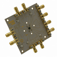
NB7L14MMNEVB
Specifications of NB7L14MMNEVB


Related parts for NB7L14MMNEVB

NB7L14MMNEVB Summary of contents
Page 1
NB7L14M 2.5V/3.3V Differential 1:4 Clock/Data Fanout Buffer/ Translator with CML Outputs and Internal Termination Description The NB7L14M is a differential 1−to−4 clock/data distribution chip with internal source terminated CML output structures, optimized for minimal skew and jitter. Device produces four identical ...
Page 2
V TCLK CLK CLK V TCLK Table 1. PIN DESCRIPTION Pin Name I − TCLK 2 CLK LVPECL, CML, LVCMOS, LVTTL, LVDS 3 CLK LVPECL, CML, LVCMOS, LVTTL, LVDS 4 V − TCLK 5,16 V Power Supply EE ...
Page 3
Table 2. ATTRIBUTES ESD Protection Moisture Sensitivity (Note 3) Flammability Rating Transistor Count Meets or exceeds JEDEC Spec EIA/JESD78 IC Latchup Test 3. For additional information, see Application Note AND8003/D. Table 3. MAXIMUM RATINGS Symbol Parameter V Positive Power Supply ...
Page 4
Table 4. DC CHARACTERISTICS, CLOCK Inputs, CML Outputs ( (Note 5) Symbol Characteristic I Power Supply Current (Inputs and Outputs Open Output HIGH Voltage (Note Output LOW Voltage (Note 6) OL Differential Input Driven Single−Ended ...
Page 5
Table 5. AC CHARACTERISTICS (V Symbol Characteristic V Output Voltage Amplitude (@V OUTPP (See Figure 4) f Maximum Operating Data Rate data t , Propagation Delay to Output Differential PLH t PHL t Duty Cycle Skew (Note 10) SKEW Within−Device ...
Page 6
DDJ = 1.6 ps* Time (80 ps/div) Figure 4. Typical Output Waveform at 2.488 Gb/s ^23 with PRBS 2 − mV) inpp *Input signal DDJ = 6.4 ps DDJ = 2 ps*** Time (18 ps/div) Figure 6. ...
Page 7
CLK CLK PLH NB7L14M Figure 9. Typical Termination for 16 mA Output Driver and Device Evaluation (Refer to Application Notes AND8020/D and AND8173/D) CLK V th CLK V th Figure 10. ...
Page 8
Table 6. INTERFACING OPTIONS INTERFACING OPTIONS CML LVDS AC−COUPLED Bias V RSECL, LVPECL LVTTL, LVCMOS An external voltage should be applied to the unused complementary differential input. Nominal voltage is 1.5 V for LVTTL and ...
Page 9
Application Information All NB7L14M inputs can accept PECL, CML, LVTTL, LVCMOS and LVDS signal levels. The limitations for differential input signal (LVDS, PECL, or CML) are PECL Driver Recommended R Values T ...
Page 10
V CC LVDS Driver LVTTL/ LVCMOS Driver V EE Figure 18. LVCMOS/LVTTL to CML Receiver Interface ORDERING INFORMATION Device NB7L14MMNG NB7L14MMNR2G †For information on tape and reel specifications, including part orientation and tape sizes, please refer ...
Page 11
... 0.05 C NOTE 3 *For additional information on our Pb−Free strategy and soldering details, please download the ON Semiconductor Soldering and Mounting Techniques Reference Manual, SOLDERRM/D. N. American Technical Support: 800−282−9855 Toll Free USA/Canada Europe, Middle East and Africa Technical Support: Phone: 421 33 790 2910 Japan Customer Focus Center Phone: 81− ...