NB4L16MMNEVB ON Semiconductor, NB4L16MMNEVB Datasheet - Page 7
NB4L16MMNEVB
Manufacturer Part Number
NB4L16MMNEVB
Description
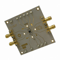
EVAL BOARD FOR NB4L16MMN
Manufacturer
ON Semiconductor
Datasheet
1.NB4L16MMNR2G.pdf
(12 pages)
Specifications of NB4L16MMNEVB
Main Purpose
Timing, Clock Buffer / Driver / Receiver / Translator
Embedded
No
Utilized Ic / Part
NB4L16M
Primary Attributes
Input Up To 5Gb/s & 3.5GHz
Secondary Attributes
Differential CML Output
Technology Type
Evaluation Board
Lead Free Status / RoHS Status
Lead free / RoHS Compliant
For Use With/related Products
NB4L16M
Other names
NB4L16MMNEVBOS


Figure 7. Typical Output Waveform at 2.488 Gb/s
Figure 9. Typical Output Waveform at 2.488 Gb/s
with PRBS 2
with PRBS 2
Figure 11. Typical Output Waveform at 5 Gb/s
with PRBS 223−1 (VINPP = 400 mV;
Input Signal DDJ = 13 ps)
Device DDJ = 1.5 ps
23
23
Device DDJ = 9 ps
−1 (V
−1 (V
Device DDJ = 1.5 ps
TIME (80 ps/div)
TIME (72 ps/div)
TIME (43 ps/div)
DDJ = 12 ps)
DDJ = 12 ps)
INPP
INPP
= 400 mV; Input Signal
= 75 mV; Input Signal
http://onsemi.com
7
Figure 12. Typical Output Waveform at 6.125 Gb/s
Figure 10. Typical Output Waveform at 3.2 Gb/s
with PRBS 2
with PRBS 2
Figure 8. Typical Output Waveform at 3.2 Gb/s
with PRBS 223−1 (VINPP = 400 mV;
Input Signal DDJ = 15 ps)
Device DDJ = 14 ps
23
^23
Device DDJ = 2 ps
−1 (V
Device DDJ = 2 ps
−1 (V
TIME (60 ps/div)
TIME (36 ps/div)
TIME (60 ps/div)
DDJ = 12 ps)
DDJ = 12 ps)
INPP
INPP
= 400 mV; Input Signal
= 75 mV; Input Signal
Related parts for NB4L16MMNEVB
Image
Part Number
Description
Manufacturer
Datasheet
Request
R

Part Number:
Description:
2.5v/3.3v, 5 Gb/s Multi Level Clock/data Input To Cml Driver / Receiver / Buffer / Translator With Internal Termination
Manufacturer:
ON Semiconductor
Datasheet:
Part Number:
Description:
ON Semiconductor [VOLTAGE REGULATOR]
Manufacturer:
ON Semiconductor
Datasheet:
Part Number:
Description:
357-036-542-201 CARDEDGE 36POS DL .156 BLK LOPRO
Manufacturer:
ON Semiconductor
Datasheet:
Part Number:
Description:
357-036-542-201 CARDEDGE 36POS DL .156 BLK LOPRO
Manufacturer:
ON Semiconductor
Datasheet:
Part Number:
Description:
357-036-542-201 CARDEDGE 36POS DL .156 BLK LOPRO
Manufacturer:
ON Semiconductor
Datasheet:
Part Number:
Description:
357-036-542-201 CARDEDGE 36POS DL .156 BLK LOPRO
Manufacturer:
ON Semiconductor
Datasheet:
Part Number:
Description:
357-036-542-201 CARDEDGE 36POS DL .156 BLK LOPRO
Manufacturer:
ON Semiconductor
Datasheet:
Part Number:
Description:
357-036-542-201 CARDEDGE 36POS DL .156 BLK LOPRO
Manufacturer:
ON Semiconductor
Datasheet:
Part Number:
Description:
357-036-542-201 CARDEDGE 36POS DL .156 BLK LOPRO
Manufacturer:
ON Semiconductor
Datasheet:
Part Number:
Description:
357-036-542-201 CARDEDGE 36POS DL .156 BLK LOPRO
Manufacturer:
ON Semiconductor
Datasheet:
Part Number:
Description:
357-036-542-201 CARDEDGE 36POS DL .156 BLK LOPRO
Manufacturer:
ON Semiconductor
Datasheet:
Part Number:
Description:
357-036-542-201 CARDEDGE 36POS DL .156 BLK LOPRO
Manufacturer:
ON Semiconductor
Datasheet:
Part Number:
Description:
Manufacturer:
ON Semiconductor
Datasheet:
Part Number:
Description:
Manufacturer:
ON Semiconductor
Datasheet: