NB4L16MMNEVB ON Semiconductor, NB4L16MMNEVB Datasheet - Page 10
NB4L16MMNEVB
Manufacturer Part Number
NB4L16MMNEVB
Description
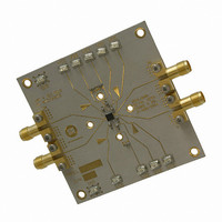
EVAL BOARD FOR NB4L16MMN
Manufacturer
ON Semiconductor
Datasheet
1.NB4L16MMNR2G.pdf
(12 pages)
Specifications of NB4L16MMNEVB
Main Purpose
Timing, Clock Buffer / Driver / Receiver / Translator
Embedded
No
Utilized Ic / Part
NB4L16M
Primary Attributes
Input Up To 5Gb/s & 3.5GHz
Secondary Attributes
Differential CML Output
Technology Type
Evaluation Board
Lead Free Status / RoHS Status
Lead free / RoHS Compliant
For Use With/related Products
NB4L16M
Other names
NB4L16MMNEVBOS


input signal (LVDS, PECL, or CML) are minimum input swing of 75 mV and the maximum input swing of 2500 mV. Within
these conditions, the input voltage can range from V
environment (Z = 50 W).
All NB4L16M inputs can accept LVPECL, CML, LVTTL, LVCMOS and LVDS signal levels. The limitations for differential
Recommended R
5.0 V 290 W
3.3 V 150 W
2.5 V 80 W
V
CC
R
T
T
Values
PECL
Driver
V
V
50 W
EE
V
CC
EE
V
CC
Figure 21. PECL to CML Receiver Interface
50 W
R
V
APPLICATION INFORMATION
Figure 20. CML to CML Interface
T
EE
Q
R
Q
T
50 W
50 W
http://onsemi.com
CC
to 1.2 V. Examples interfaces are illustrated below in a 50 W
Z
Z
10
Z
Z
V
V
BIAS
BIAS
V
V
CC
CC
V
V
V
V
TD
TD
TD
TD
D
D
D
D
50 W
50 W
V
V
50 W
50 W
EE
EE
V
V
CC
CC
Related parts for NB4L16MMNEVB
Image
Part Number
Description
Manufacturer
Datasheet
Request
R

Part Number:
Description:
2.5v/3.3v, 5 Gb/s Multi Level Clock/data Input To Cml Driver / Receiver / Buffer / Translator With Internal Termination
Manufacturer:
ON Semiconductor
Datasheet:
Part Number:
Description:
ON Semiconductor [VOLTAGE REGULATOR]
Manufacturer:
ON Semiconductor
Datasheet:
Part Number:
Description:
357-036-542-201 CARDEDGE 36POS DL .156 BLK LOPRO
Manufacturer:
ON Semiconductor
Datasheet:
Part Number:
Description:
357-036-542-201 CARDEDGE 36POS DL .156 BLK LOPRO
Manufacturer:
ON Semiconductor
Datasheet:
Part Number:
Description:
357-036-542-201 CARDEDGE 36POS DL .156 BLK LOPRO
Manufacturer:
ON Semiconductor
Datasheet:
Part Number:
Description:
357-036-542-201 CARDEDGE 36POS DL .156 BLK LOPRO
Manufacturer:
ON Semiconductor
Datasheet:
Part Number:
Description:
357-036-542-201 CARDEDGE 36POS DL .156 BLK LOPRO
Manufacturer:
ON Semiconductor
Datasheet:
Part Number:
Description:
357-036-542-201 CARDEDGE 36POS DL .156 BLK LOPRO
Manufacturer:
ON Semiconductor
Datasheet:
Part Number:
Description:
357-036-542-201 CARDEDGE 36POS DL .156 BLK LOPRO
Manufacturer:
ON Semiconductor
Datasheet:
Part Number:
Description:
357-036-542-201 CARDEDGE 36POS DL .156 BLK LOPRO
Manufacturer:
ON Semiconductor
Datasheet:
Part Number:
Description:
357-036-542-201 CARDEDGE 36POS DL .156 BLK LOPRO
Manufacturer:
ON Semiconductor
Datasheet:
Part Number:
Description:
357-036-542-201 CARDEDGE 36POS DL .156 BLK LOPRO
Manufacturer:
ON Semiconductor
Datasheet:
Part Number:
Description:
Manufacturer:
ON Semiconductor
Datasheet:
Part Number:
Description:
Manufacturer:
ON Semiconductor
Datasheet: