NCP5104BA36WGEVB ON Semiconductor, NCP5104BA36WGEVB Datasheet - Page 4
NCP5104BA36WGEVB
Manufacturer Part Number
NCP5104BA36WGEVB
Description
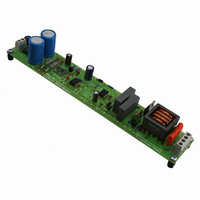
EVAL BOARD FOR NCP5104BA36WG
Manufacturer
ON Semiconductor
Datasheets
1.NCP5104DR2G.pdf
(15 pages)
2.NCP5104BA36WGEVB.pdf
(3 pages)
3.NCP5104BA36WGEVB.pdf
(6 pages)
Specifications of NCP5104BA36WGEVB
Design Resources
NCP5104 Demo Board BOM NCP5104BAL36WEVB Gerber Files NCP5104 Demo Board Schematic
Main Purpose
Lighting, Ballast Control
Embedded
No
Utilized Ic / Part
NCP5104
Primary Attributes
Output Power 36W, PL-L Type
Secondary Attributes
Input Range 85 ~ 145 Vac or 184 ~ 265 Vac
Silicon Manufacturer
On Semiconductor
Silicon Core Number
NCP5104
Kit Application Type
Lighting
Application Sub Type
Ballast
Development Tool Type
Hardware - Eval/Demo Board
Rohs Compliant
Yes
Leaded Process Compatible
Yes
Lead Free Status / RoHS Status
Lead free / RoHS Compliant
For Use With/related Products
NCP5104BA36WG
Other names
NCP5104BA36WGEVBOS


1. Parameter guaranteed by design.
2. T
3. Turn−off propagation delay @ Vbridge = 600 V is guaranteed by design.
4. See characterization curve for Dt parameters variation on the full range temperature.
5. Timing diagram definition see: Figure 4, Figure 5 and Figure 6.
Output high short circuit pulsed current V
Output low short circuit pulsed current V
Output resistor (Typical value @ 25°C) Source
Output resistor (Typical value @ 25°C) Sink
High level output voltage, V
Low level output voltage V
Turn−on propagation delay (Vbridge = 0 V) (Note 2)
Turn−off propagation delay (Vbridge = 0 V or 50 V) (Note 3)
Shutdown propagation delay, when Shutdown is enabled
Shutdown propagation delay, when Shutdown is disabled
Output voltage rise time (from 10% to 90% @ V
Output voltage fall time (from 90% to 10% @ V
Propagation delay matching between the High side and the Low side
@ 25°C (Note 4)
Internal fixed dead time (Note 5)
Low level input voltage threshold
Input pull−down resistor (V
High level input voltage threshold
Logic “1” input bias current @ V
Logic “0” input bias current @ V
Vcc UV Start−up voltage threshold
Vcc UV Shut−down voltage threshold
Hysteresis on Vcc
Vboot Start−up voltage threshold reference to bridge pin
(Vboot_stup = Vboot − Vbridge)
Vboot UV Shut−down voltage threshold
Hysteresis on Vboot
Leakage current on high voltage pins to GND
(V
Consumption in active mode (Vcc = Vboot, fsw = 100 kHz and 1 nF load on
both driver outputs)
Consumption in inhibition mode (Vcc = Vboot)
Vcc current consumption in inhibition mode
Vboot current consumption in inhibition mode
ELECTRICAL CHARACTERISTIC
OUTPUT SECTION
DYNAMIC OUTPUT SECTION
INPUT SECTION
SUPPLY SECTION
BOOT
ON
= T
= V
OFF
BRIDGE
+ DT
= DRV_HI = 600 V)
DRV_XX
IN
BIAS
< 0.5 V)
−V
IN
IN
@ I
= 5 V @ 25°C
= 0 V @ 25°C
DRV_XX
Rating
DRV_XX
DRV
(V
DRV
@ I
CC
= Vcc, PW v 10 ms (Note 1)
= 0 V, PW v 10 ms (Note 1)
= 20 mA
DRV_XX
= V
CC
CC
boot
= 15 V) with 1 nF load
= 15 V) with 1 nF load
= 15 V, V
= 20 mA
http://onsemi.com
GND
= V
4
bridge
, −40°C < T
Vboot_shtdwn
Vboot_shtdwn
Vcc_shtdwn
Vboot_stup
I
Vcc_stup
Vcc_hyst
DRVsource
I
Symbol
I
V
HV_LEAK
V
DRVsink
t
t
ICC1
ICC2
ICC3
ICC4
sd_dis
DRV_H
sd_en
R
R
DRV_L
t
t
V
R
V
I
I
OFF
DT
ON
Dt
IN+
IN−
OH
t
t
OL
IN
IN
IN
r
f
J
< 125°C, Outputs loaded with 1 nF)
Min
400
2.3
8.0
7.3
0.3
8.0
7.3
0.3
−
−
−
−
−
−
−
−
−
−
−
−
−
−
−
−
−
−
−
−
−
−
T
J
−40°C to 125°C
Typ
250
500
620
100
100
620
520
200
250
200
0.7
0.2
8.9
8.2
0.7
8.9
8.2
0.7
30
10
85
35
10
50
−
−
5
−
5
4
Max
800
170
170
800
160
650
400
1.6
0.6
0.8
2.0
9.8
9.0
9.8
9.0
60
20
75
45
25
40
−
−
−
−
−
−
5
−
−
Units
mA
mA
mA
kW
mA
mA
mA
mA
mA
mA
ns
ns
ns
ns
ns
ns
ns
ns
W
W
V
V
V
V
V
V
V
V
V
V
Related parts for NCP5104BA36WGEVB
Image
Part Number
Description
Manufacturer
Datasheet
Request
R

Part Number:
Description:
Half Bridge Driver
Manufacturer:
ON Semiconductor
Datasheet:
Part Number:
Description:
ON Semiconductor [VOLTAGE REGULATOR]
Manufacturer:
ON Semiconductor
Datasheet:
Part Number:
Description:
357-036-542-201 CARDEDGE 36POS DL .156 BLK LOPRO
Manufacturer:
ON Semiconductor
Datasheet:
Part Number:
Description:
357-036-542-201 CARDEDGE 36POS DL .156 BLK LOPRO
Manufacturer:
ON Semiconductor
Datasheet:
Part Number:
Description:
357-036-542-201 CARDEDGE 36POS DL .156 BLK LOPRO
Manufacturer:
ON Semiconductor
Datasheet:
Part Number:
Description:
357-036-542-201 CARDEDGE 36POS DL .156 BLK LOPRO
Manufacturer:
ON Semiconductor
Datasheet:
Part Number:
Description:
357-036-542-201 CARDEDGE 36POS DL .156 BLK LOPRO
Manufacturer:
ON Semiconductor
Datasheet:
Part Number:
Description:
357-036-542-201 CARDEDGE 36POS DL .156 BLK LOPRO
Manufacturer:
ON Semiconductor
Datasheet:
Part Number:
Description:
357-036-542-201 CARDEDGE 36POS DL .156 BLK LOPRO
Manufacturer:
ON Semiconductor
Datasheet:
Part Number:
Description:
357-036-542-201 CARDEDGE 36POS DL .156 BLK LOPRO
Manufacturer:
ON Semiconductor
Datasheet:
Part Number:
Description:
357-036-542-201 CARDEDGE 36POS DL .156 BLK LOPRO
Manufacturer:
ON Semiconductor
Datasheet:
Part Number:
Description:
357-036-542-201 CARDEDGE 36POS DL .156 BLK LOPRO
Manufacturer:
ON Semiconductor
Datasheet:
Part Number:
Description:
Manufacturer:
ON Semiconductor
Datasheet:
Part Number:
Description:
Manufacturer:
ON Semiconductor
Datasheet: