NCP5104BA36WGEVB ON Semiconductor, NCP5104BA36WGEVB Datasheet - Page 3
NCP5104BA36WGEVB
Manufacturer Part Number
NCP5104BA36WGEVB
Description
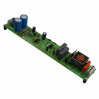
EVAL BOARD FOR NCP5104BA36WG
Manufacturer
ON Semiconductor
Datasheets
1.NCP5104DR2G.pdf
(15 pages)
2.NCP5104BA36WGEVB.pdf
(3 pages)
3.NCP5104BA36WGEVB.pdf
(6 pages)
Specifications of NCP5104BA36WGEVB
Design Resources
NCP5104 Demo Board BOM NCP5104BAL36WEVB Gerber Files NCP5104 Demo Board Schematic
Main Purpose
Lighting, Ballast Control
Embedded
No
Utilized Ic / Part
NCP5104
Primary Attributes
Output Power 36W, PL-L Type
Secondary Attributes
Input Range 85 ~ 145 Vac or 184 ~ 265 Vac
Silicon Manufacturer
On Semiconductor
Silicon Core Number
NCP5104
Kit Application Type
Lighting
Application Sub Type
Ballast
Development Tool Type
Hardware - Eval/Demo Board
Rohs Compliant
Yes
Leaded Process Compatible
Yes
Lead Free Status / RoHS Status
Lead free / RoHS Compliant
For Use With/related Products
NCP5104BA36WG
Other names
NCP5104BA36WGEVBOS


Stresses exceeding Maximum Ratings may damage the device. Maximum Ratings are stress ratings only. Functional operation above the
Recommended Operating Conditions is not implied. Extended exposure to stresses above the Recommended Operating Conditions may affect
device reliability.
MAXIMUM RATINGS
V
BOOT−
V
dV
CC_transient
V
V
V
V
V
Rating
V
BRIDGE
T
BRIDGE
BRIDGE
DRV_LO
IN
DRV_HI
R
V
J_max
BOOT
T
, V
qJA
CC
ST
V
BRIDGE
SD
/dt
Á Á Á Á Á Á Á
Á Á Á Á Á Á Á
Á Á Á Á Á Á Á
Á Á Á Á Á Á Á
Á Á Á Á Á Á Á
Á Á Á Á Á Á Á
Á Á Á Á Á Á Á
Á Á Á Á Á Á Á
Á Á Á Á Á Á Á
Á Á Á Á Á Á Á
Á Á Á Á Á Á Á
Á Á Á Á Á Á Á
Á Á Á Á Á Á Á
Á Á Á Á Á Á Á
Á Á Á Á Á Á Á
Á Á Á Á Á Á Á
PIN DESCRIPTION
Main power supply voltage
Main transient power supply voltage:
VHV: High Voltage BRIDGE pin
Allowable Negative Bridge Pin Voltage for IN Signal Propagation to DRV_LO
VHV: Floating supply voltage
VHV: High side output voltage
Low side output voltage
Allowable output slew rate
Inputs IN & SD
ESD Capability:
− HBM model (all pins except pins 6−7−8 in 8)
− Machine model (all pins except pins 6−7−8)
Latch up capability per JEDEC JESD78
Power dissipation and Thermal characteristics
PDIP−8: Thermal Resistance, Junction−to−Air
SO−8: Thermal Resistance, Junction−to−Air
Storage Temperature Range
Maximum Operating Junction Temperature
V
IN
SD
GND
DRV_LO
V
DRV_HI
BRIDGE
VHV: High Voltage BOOT Pin
CC
BOOT
IV
CC_max
Pin Name
= 5 mA during 10 ms
Á Á Á Á Á Á Á Á Á Á Á Á Á Á Á Á Á
Á Á Á Á Á Á Á Á Á Á Á Á Á Á Á Á Á
Á Á Á Á Á Á Á Á Á Á Á Á Á Á Á Á Á
Á Á Á Á Á Á Á Á Á Á Á Á Á Á Á Á Á
Á Á Á Á Á Á Á Á Á Á Á Á Á Á Á Á Á
Á Á Á Á Á Á Á Á Á Á Á Á Á Á Á Á Á
Á Á Á Á Á Á Á Á Á Á Á Á Á Á Á Á Á
Á Á Á Á Á Á Á Á Á Á Á Á Á Á Á Á Á
Á Á Á Á Á Á Á Á Á Á Á Á Á Á Á Á Á
Á Á Á Á Á Á Á Á Á Á Á Á Á Á Á Á Á
Á Á Á Á Á Á Á Á Á Á Á Á Á Á Á Á Á
Á Á Á Á Á Á Á Á Á Á Á Á Á Á Á Á Á
Á Á Á Á Á Á Á Á Á Á Á Á Á Á Á Á Á
Á Á Á Á Á Á Á Á Á Á Á Á Á Á Á Á Á
Á Á Á Á Á Á Á Á Á Á Á Á Á Á Á Á Á
Á Á Á Á Á Á Á Á Á Á Á Á Á Á Á Á Á
Low Side and Main Power Supply
Logic Input
Logic Input for Shutdown
Ground
Low Side Gate Drive Output
Bootstrap Power Supply
High Side Gate Drive Output
Bootstrap Return or High Side Floating Supply Return
Symbol
http://onsemi.com
3
Description
−0.3 to V
−1.0 to V
V
BRIDGE
V
−55 to +150
−0.3 to 20
−0.3 to 20
−1 to 620
−1 to 600
BOOT
Value
+150
−10
200
100
178
23
50
2
CC
CC
− 0.3 to
+ 0.3
+ 0.3
+ 0.3
°C/W
V/ns
Unit
kV
°C
°C
V
V
V
V
V
V
V
V
V
V
Related parts for NCP5104BA36WGEVB
Image
Part Number
Description
Manufacturer
Datasheet
Request
R

Part Number:
Description:
Half Bridge Driver
Manufacturer:
ON Semiconductor
Datasheet:
Part Number:
Description:
ON Semiconductor [VOLTAGE REGULATOR]
Manufacturer:
ON Semiconductor
Datasheet:
Part Number:
Description:
357-036-542-201 CARDEDGE 36POS DL .156 BLK LOPRO
Manufacturer:
ON Semiconductor
Datasheet:
Part Number:
Description:
357-036-542-201 CARDEDGE 36POS DL .156 BLK LOPRO
Manufacturer:
ON Semiconductor
Datasheet:
Part Number:
Description:
357-036-542-201 CARDEDGE 36POS DL .156 BLK LOPRO
Manufacturer:
ON Semiconductor
Datasheet:
Part Number:
Description:
357-036-542-201 CARDEDGE 36POS DL .156 BLK LOPRO
Manufacturer:
ON Semiconductor
Datasheet:
Part Number:
Description:
357-036-542-201 CARDEDGE 36POS DL .156 BLK LOPRO
Manufacturer:
ON Semiconductor
Datasheet:
Part Number:
Description:
357-036-542-201 CARDEDGE 36POS DL .156 BLK LOPRO
Manufacturer:
ON Semiconductor
Datasheet:
Part Number:
Description:
357-036-542-201 CARDEDGE 36POS DL .156 BLK LOPRO
Manufacturer:
ON Semiconductor
Datasheet:
Part Number:
Description:
357-036-542-201 CARDEDGE 36POS DL .156 BLK LOPRO
Manufacturer:
ON Semiconductor
Datasheet:
Part Number:
Description:
357-036-542-201 CARDEDGE 36POS DL .156 BLK LOPRO
Manufacturer:
ON Semiconductor
Datasheet:
Part Number:
Description:
357-036-542-201 CARDEDGE 36POS DL .156 BLK LOPRO
Manufacturer:
ON Semiconductor
Datasheet:
Part Number:
Description:
Manufacturer:
ON Semiconductor
Datasheet:
Part Number:
Description:
Manufacturer:
ON Semiconductor
Datasheet: