STEVAL-IHM021V2 STMicroelectronics, STEVAL-IHM021V2 Datasheet
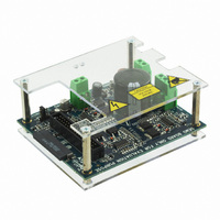
STEVAL-IHM021V2
Specifications of STEVAL-IHM021V2


Related parts for STEVAL-IHM021V2


STEVAL-IHM021V2 Summary of contents
Page 1
N-channel 525 V, 1.28 Ω, 4.4 A, DPAK, TO-220FP Features R DS(on) Type V DSS max < 1.5 Ω STD5N52U 525 V < 1.5 Ω STF5N52U 525 V ■ 100% avalanche tested ■ Outstanding dv/dt capability ■ Gate charge minimized ...
Page 2
Contents Contents 1 Electrical ratings . . . . . . . . . . . . . . . . . . . . . . . . . . . . . . . . . . . ...
Page 3
STF5N52U, STD5N52U 1 Electrical ratings Table 2. Absolute maximum ratings Symbol V Gate- source voltage GS I Drain current (continuous Drain current (continuous (1) I Drain current (pulsed Total dissipation at ...
Page 4
Electrical characteristics 2 Electrical characteristics (Tcase =25 °C unless otherwise specified) Table 4. On /off states Symbol Drain-source V (BR)DSS breakdown voltage Zero gate voltage I DSS drain current (V Gate-body leakage I GSS current (V V Gate threshold voltage ...
Page 5
STF5N52U, STD5N52U Table 7. Source drain diode Symbol I Source-drain current SD (1) I Source-drain current (pulsed) SDM (2) V Forward on voltage SD t Reverse recovery time rr Q Reverse recovery charge rr I Reverse recovery current RRM t ...
Page 6
Electrical characteristics 2.1 Electrical characteristics (curves) Figure 2. Safe operating area for TO-220FP Figure 4. Safe operating area for DPAK Figure 6. Output characteristics 6/15 Figure 3. Thermal impedance for TO-220FP Figure 5. Thermal impedance for DPAK Figure 7. Transfer ...
Page 7
STF5N52U, STD5N52U Figure 8. Normalized BV DSS Figure 10. Gate charge vs gate-source voltage Figure 12. Normalized gate threshold voltage vs temperature vs temperature Figure 9. Figure 11. Capacitance variations Figure 13. Normalized on resistance vs Doc ID 15684 Rev ...
Page 8
Electrical characteristics Figure 14. Source-drain diode forward characteristics 8/15 Figure 15. Maximum avalanche energy vs temperature Doc ID 15684 Rev 1 STF5N52U, STD5N52U ...
Page 9
STF5N52U, STD5N52U 3 Test circuits Figure 16. Switching times test circuit for resistive load D.U. Figure 18. Test circuit for inductive load switching and diode recovery times ...
Page 10
Package mechanical data 4 Package mechanical data In order to meet environmental requirements, ST offers these devices in different grades of ® ECOPACK packages, depending on their level of environmental compliance. ECOPACK specifications, grade definitions and product status are available ...
Page 11
STF5N52U, STD5N52U DIM TO-252 (DPAK) mechanical data mm ...
Page 12
Package mechanical data Dim 12/15 TO-220FP mechanical data ...
Page 13
STF5N52U, STD5N52U 5 Packaging mechanical data DPAK FOOTPRINT All dimensions are in millimeters TAPE MECHANICAL DATA mm DIM. MIN. MAX. A0 6 1.5 D1 1.5 E 1.65 F 7.4 K0 2.55 P0 3.9 P1 7.9 P2 ...
Page 14
Revision history 6 Revision history Table 9. Document revision history Date 06-May-2009 14/15 Revision 1 First release Doc ID 15684 Rev 1 STF5N52U, STD5N52U Changes ...
Page 15
... STF5N52U, STD5N52U Information in this document is provided solely in connection with ST products. STMicroelectronics NV and its subsidiaries (“ST”) reserve the right to make changes, corrections, modifications or improvements, to this document, and the products and services described herein at any time, without notice. All ST products are sold pursuant to ST’s terms and conditions of sale. ...