CY3275 Cypress Semiconductor Corp, CY3275 Datasheet - Page 15
CY3275
Manufacturer Part Number
CY3275
Description
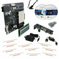
KIT DEV POWERLINE PROGRAM
Manufacturer
Cypress Semiconductor Corp
Type
Other Power Managementr
Specifications of CY3275
Main Purpose
Interface, Transceiver, Powerline Communication
Embedded
No
Utilized Ic / Part
CY8CPLC20
Primary Attributes
2400bps Data Transfer Over Low Voltage Power Lines
Secondary Attributes
User Configurable LEDs
Board Size
101.6 mm x 101.6 mm
Interface Type
RS-232, Ethernet, I2C, ISSP
Maximum Operating Temperature
+ 40 C
Operating Supply Voltage
12 V, 24 V
Product
Power Management Development Tools
Dimensions
101.6 mm x 101.6 mm
Silicon Manufacturer
Cypress
Silicon Core Number
CY8CPLC20
Kit Application Type
Communication & Networking
Application Sub Type
Low Voltage Powerline Communication
Rohs Compliant
Yes
For Use With/related Products
CY8CPLC20
Lead Free Status / RoHS Status
Lead free / RoHS Compliant
Lead Free Status / RoHS Status
Lead free / RoHS Compliant, Lead free / RoHS Compliant
Other names
428-3005


2.3.4.3
CY3275 Cypress Low Voltage Programmable PLC Development Kit Guide, Doc. # 001-53657 Rev. *B
Potentiometer and DIP Switches
There are 8-bit general purpose dip switches (S3) provided for the user. A general purpose potenti-
ometer (R47) is provided next to the dip switches. This potentiometer can be routed to the chip using
the GPIO pins. The second potentiometer (R46) is specifically meant to control the contrast for the
LCD daughter card in the LCD1 slot.
Figure 2-4. Dip Switches
Key components and their use:
J15
S3[7-0]
Potentiometer [R47]
LCD Contrast[R46]
Headers and Jumpers
Component
V - Vdd pin: This pin can provide a maximum of 50 mA at 5V to an external
board only when the input to the board is 12V. For input voltages greater
than 12V do not use this pin to power another board. This pin is only to
source the current. DO NOT SUPPLY POWER TO THIS PIN FOR POWERING
THE CY8CPLC20 DEVICE. Note that the PWR jumper (JP1) needs to be con-
nected to enable this functionality.
G - Gnd Pin: This pin can provide the ground reference to an external board.
This pin connects to the ground pin of the external board.
D - I2C Data (SDA): This is the data line for the I2C communication. This pin
is directly connected to the CY8CPLC20 device
C - I2C Clock (SCL): This is the clock line for the I2C communication. This
pin is directly connected to the CY8CPLC20 device.
R – Reset: Connecting this pin to an external board enables the
CY8CPLC20 chip to be reset by an external board. Note that the RES
jumper needs to be connected for enabling this functionality.
These dip switches are general purpose and can be routed to any port of
the CY8CPLC20 chip.
This is a variable resistor that connects to the VR header. It can be used to
generate a voltage between +5V and GND.
Adjusting this potentiometer adjusts the contrast on the LCD Daughter
Card.
Description
Description
PLC LV Development Board
15
[+] Feedback
Related parts for CY3275
Image
Part Number
Description
Manufacturer
Datasheet
Request
R

Part Number:
Description:
Manufacturer:
Cypress Semiconductor Corp
Datasheet:
Part Number:
Description:
Manufacturer:
Cypress Semiconductor Corp
Datasheet:
Part Number:
Description:
Manufacturer:
Cypress Semiconductor Corp
Datasheet:
Part Number:
Description:
Manufacturer:
Cypress Semiconductor Corp
Datasheet:
Part Number:
Description:
Manufacturer:
Cypress Semiconductor Corp
Datasheet: