CDB8416 Cirrus Logic Inc, CDB8416 Datasheet - Page 7
CDB8416
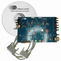
Manufacturer Part Number
CDB8416
Description
BOARD EVAL FOR CS8416 RCVR
Manufacturer
Cirrus Logic Inc
Datasheet
1.CDB8416.pdf
(26 pages)
Specifications of CDB8416
Main Purpose
Audio, Audio Processing
Embedded
Yes, Other
Utilized Ic / Part
CS8406, CS8416
Primary Attributes
Digital Audio Transmitter and Receiver
Secondary Attributes
Graphic User Interface, AES/EBU, S/PDIF and EIAJ-340
Product
Audio Modules
Silicon Manufacturer
Cirrus Logic
Silicon Core Number
CS8416
Kit Application Type
Communication & Networking
Application Sub Type
Digital Audio Receiver
Kit Contents
Board
Rohs Compliant
No
Lead Free Status / RoHS Status
Contains lead / RoHS non-compliant
Lead Free Status / RoHS Status
Lead free / RoHS Compliant, Contains lead / RoHS non-compliant
Other names
598-1017


3. BOARD SETUP
3.1
1) Verify that all power supplies are off before
2) Connect a +3.3 V DC power supply to the
3) Connect a +3.3 V to +5.0 V DC power supply
4) Connect a +5.0 V DC power supply to the +5 V
5) Connect the common ground of the power sup-
6) Apply power to the board. D9 should illumi-
3.2
1) Place switch S1-H/S in the OPEN position.
2) Place switches S3-INPUT, S3-8416_PCM, S3-
3) Press and release the RESET switch S3. The
3.3
1) Place switch S1-H/S in the CLOSED position.
2) Place switches S1-M/S, S3-INPUT, S3-
DS578DB3
making connections.
VD+/VA+ (J6) binding post and place jumper
J8 in the ADJUST position. This connection
may be omitted by setting J8 to the REG posi-
tion. VD+/VA+ will be derived from the on-
board +3.3V regulator.
to the VL+ (J5) binding post and place jumper
J7 in the ADJUST position. This connection
may be omitted by setting J7 to the +5 V posi-
tion. VL+ will be derived from the +5 V bind-
ing post.
(J3) binding post.
plies to the GND (J4) binding post.
nate indicating power is applied to VD+/VA+.
NVSEL,
TXSEL1, S3-TXSEL0, S1-M/S, S1-SFMT1,
S1-SFMT0, S4-8406_PCM, S4-TCBLD, S4-
CEN to the appropriate positions.
board should now be setup for use in Hardware
Mode.
8416_PCM, and S4-8406_PCM to the appro-
priate positions. All other switch setting do not
Power Supplies:
Hardware Mode Settings:
Software Mode Settings:
S3-RXSEL1,
S3-RXSEL0,
S3-
3) Press and release the RESET switch S2. The
4) Connect a DB-25 parallel port cable from the
3.3.1
1) Create a directory called CDB8416 anywhere
2) Copy CDB8416.exe from the included CD into
3) Run port95nt.exe from the CD. After running
4) If desired, create a shortcut to CDB8416.exe on
5) Double-click on CDB8416.exe or its shortcut.
6) Click on the button on the lower right labeled
7) Select the LPT port you are using to connect to
8) Shut down the application, reset the board, and
3.3.2
1) In the “CS8416 AES Receiver Controls” win-
2) In the “CS8406 AES Transmitter Controls”
3) In the “CS8416 AES Receiver Controls” win-
effect Software Mode operation.
board should now be setup for use in Software
mode.
PC’s parallel port to J1 on the CDB8416.
on your system.
this directory.
the program the system will need to be restart-
ed.
your desktop. You should now be able to run
CDB8416.exe.
“Advanced”.
the CDB8416.
then restart the application.
dow, select the check box “Enable Internal
Clocks” (enables the RUN bit in the Clock
Control register).
window, select the check box “Enable Clocks”
(enables the RUN bit in the Clock Control reg-
ister).
dow,
SCLK/LRCK”. Make sure that switch S1-M/S
is in the OPEN position.
Installing the Software:
Verifying Board Operation:
select
the
check
box
CDB8416
“Generate
7
Related parts for CDB8416
Image
Part Number
Description
Manufacturer
Datasheet
Request
R

Part Number:
Description:
Development Kit
Manufacturer:
Cirrus Logic Inc
Datasheet:
Part Number:
Description:
Development Kit
Manufacturer:
Cirrus Logic Inc
Datasheet:


Part Number:
Description:
High-efficiency PFC + Fluorescent Lamp Driver Reference Design
Manufacturer:
Cirrus Logic Inc
Datasheet:
Part Number:
Description:
Development Kit
Manufacturer:
Cirrus Logic Inc
Datasheet:
Part Number:
Description:
Development Kit
Manufacturer:
Cirrus Logic Inc
Datasheet:

Part Number:
Description:
Development Kit
Manufacturer:
Cirrus Logic Inc
Datasheet:
Part Number:
Description:
Development Kit
Manufacturer:
Cirrus Logic Inc
Datasheet:
Part Number:
Description:
Development Kit
Manufacturer:
Cirrus Logic Inc
Datasheet:
Part Number:
Description:
Development Kit
Manufacturer:
Cirrus Logic Inc
Datasheet:

Part Number:
Description:
EVALUATION BOARD FOR CS8427
Manufacturer:
Cirrus Logic Inc
Datasheet:

Part Number:
Description:
EVALUATION BOARD FOR CS8420
Manufacturer:
Cirrus Logic Inc
Datasheet:

Part Number:
Description:
KIT DEVELOPMENT EP9315 ARM9
Manufacturer:
Cirrus Logic Inc
Datasheet:

Part Number:
Description:
KIT DEVELOPMENT EP9302 ARM9
Manufacturer:
Cirrus Logic Inc
Datasheet:

Part Number:
Description:
KIT DEVELOPMENT EP9307 ARM9
Manufacturer:
Cirrus Logic Inc
Datasheet: