AD9958/PCBZ Analog Devices Inc, AD9958/PCBZ Datasheet - Page 3
AD9958/PCBZ
Manufacturer Part Number
AD9958/PCBZ
Description
BOARD EVALUATION FOR AD9958
Manufacturer
Analog Devices Inc
Series
AgileRF™r
Specifications of AD9958/PCBZ
Design Resources
Low Jitter Sampling Clock Generator for High Performance ADCs Using AD9958/9858 and AD9515 (CN0109) Phase Coherent FSK Modulator (CN0186)
Main Purpose
Timing, Direct Digital Synthesis (DDS)
Embedded
No
Utilized Ic / Part
AD9958
Primary Attributes
10-Bit DAC, 32-Bit Tuning Word Width
Secondary Attributes
500MHz, Graphical User Interface, 2-Channel
Lead Free Status / RoHS Status
Lead free / RoHS Compliant
Available stocks
Company
Part Number
Manufacturer
Quantity
Price
Company:

Part Number:
AD9958/PCBZ
Manufacturer:
Analog Devices Inc
Quantity:
135


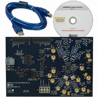
EVALUATION BOARD HARDWARE
PACKAGE CONTENTS
The AD9958/PCB kit contains the following items:
•
•
REQUIREMENTS
In order to successfully use the evaluation board and run the
software, the requirements listed in Table 1 must be met.
Table 1. AD9958/PCB Requirements
Item
Operating System
Processor
Memory
Ports
Clocking
Power Supplies
Measurement
Cables
SETTING UP THE EVALUATION BOARD
Powering the Part
The AD9958 evaluation board has five power supply
connectors: TB1, J10, J16, J18, and J20. TB1 powers the DDS,
the PC interface logic, and the USB circuitry. J10 powers the
input clock circuitry. J18 provides the reference voltage needed
for band gap functionality. J16 and J20 power the analog
circuitry of individual DACs. It is important to keep in mind
that the AD9958 evaluation board has been preconfigured so
that these two AVDD connections are tied together. Supplying
power to any one of the AVDD connections (J16 or J20) allows
for the proper functionality of the analog circuitry of both
DACs. Table 2 shows the necessary connections and the
appropriate biasing voltage.
AD9958 evaluation board
AD9958/PCB installation software
Requirement
Windows® 98/Windows® ME/
Windows® 2000/Windows® XP
Pentium® I or better
128 MB or better
One USB port
Signal generator capable of generating
sinusoidal waves of at least 3 dBm power,
up to at least 10 MHz
Capability to generate at least two
independent dc voltages (1.8 V/3.3 V)
Appropriate measurement device, such as
a spectrum analyzer or a high bandwidth
oscilloscope
USB 1.1/2.0 cable, and SMA-to-X cables
(X = SMA or BNC, depending on the
connector of the device interfacing with
the board)
Rev. 0 | Page 3 of 28
Table 2. Connections and Biasing Voltage
Connector
TB1
TB1
TB1
TB1
J10
J16
J18
J20
Note that the AD9958/PCB is preconfigured so that the
CLK_VDD, BG_VDD, and all other AVDD connections are
tied together. Therefore, only one connection (J10, J16, J18, or
J20) needs power for proper functionality of the two channels.
These AVDD connections can be separated for better channel
isolation. This is accomplished by removing the 0 Ω resistors
(R21, R32 to R51, R54 to R64), which tie the planes together,
found on the back of the evaluation board. When doing this, be
sure that CLK_VDD, BG_VDD, and the AVDD connection for
all desired channel(s) are powered.
Clocking the Part
The AD9958 architecture provides the user with two options when
providing an input signal to the part. Figure 1 shows that the user
can clock the frequency synthesizer/DDS directly by connecting
an external clocking signal to the REF_CLK connector, J9, or by
providing an external crystal. Place Jumper W11 on REF_CLK
to use the external clocking option. To use an external crystal as
the clocking source, place Jumper W11 on CRYSTAL.
Please refer to the AD9958 data sheet for details on the maximum
input speeds and input sensitivities of these two inputs.
Communicating with the Part
Two interface standards are available on the evaluation board:
•
•
Analog Devices provides a GUI for the PC; it does not provide
control software for external controllers.
Use the jumper settings listed in Table 3 to enable different
modes of communication.
Table 3. Jumper Settings for Communication Modes
Mode
PC control, USB port
External control
USB 1.1/2.0 interface
Header row (U2, U13), which places the part under the
control of an external controller (such as a µP, FPGA, or DSP)
Pin No.
1
2
3
4
Settings
Set W7 to PC. Place a jumper on W1,
W2, W3, W9, and W10.
Set W7 to manual. Place a jumper on
W9, and remove W1, W2, W3, and W10
(or leave it stored as a shunt).
Label
VCC_USB
DVDD_I/O
GND
DVDD
CLK_VDD
AVDD
BG_VDD
AVDD
AD9958/PCB
Voltage (V)
3.3
3.3
0
1.8
1.8
1.8
1.8
1.8
Related parts for AD9958/PCBZ
Image
Part Number
Description
Manufacturer
Datasheet
Request
R

Part Number:
Description:
BOARD EVALUATION FOR AD9958
Manufacturer:
Analog Devices Inc
Datasheet:


Part Number:
Description:
±1.7g Dual-Axis IMEMS Accelerometer Evaluation Board
Manufacturer:
Analog Devices Inc
Datasheet:

Part Number:
Description:
Inertial Sensor Evaluation System
Manufacturer:
Analog Devices Inc
Datasheet:
Part Number:
Description:
Manufacturer:
Analog Devices Inc
Datasheet:
Part Number:
Description:
Manufacturer:
Analog Devices Inc
Datasheet:
Part Number:
Description:
Manufacturer:
Analog Devices Inc
Datasheet:
Part Number:
Description:
Manufacturer:
Analog Devices Inc
Datasheet:
Part Number:
Description:
Manufacturer:
Analog Devices Inc
Datasheet:
Part Number:
Description:
Manufacturer:
Analog Devices Inc
Datasheet:
Part Number:
Description:
Manufacturer:
Analog Devices Inc
Datasheet:
Part Number:
Description:
Manufacturer:
Analog Devices Inc
Datasheet:
Part Number:
Description:
Manufacturer:
Analog Devices Inc
Datasheet: