AD9958/PCBZ Analog Devices Inc, AD9958/PCBZ Datasheet - Page 15
AD9958/PCBZ
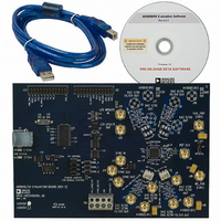
Manufacturer Part Number
AD9958/PCBZ
Description
BOARD EVALUATION FOR AD9958
Manufacturer
Analog Devices Inc
Series
AgileRF™r
Specifications of AD9958/PCBZ
Design Resources
Low Jitter Sampling Clock Generator for High Performance ADCs Using AD9958/9858 and AD9515 (CN0109) Phase Coherent FSK Modulator (CN0186)
Main Purpose
Timing, Direct Digital Synthesis (DDS)
Embedded
No
Utilized Ic / Part
AD9958
Primary Attributes
10-Bit DAC, 32-Bit Tuning Word Width
Secondary Attributes
500MHz, Graphical User Interface, 2-Channel
Lead Free Status / RoHS Status
Lead free / RoHS Compliant
Available stocks
Company
Part Number
Manufacturer
Quantity
Price
Company:

Part Number:
AD9958/PCBZ
Manufacturer:
Analog Devices Inc
Quantity:
135


In the linear sweep mode of operation, only the first Profile
Register field (Frequency 01, Phase 01, or Amplitude 01) is
used. It indicates the ending point of the sweep. In Figure 28,
the frequency linear sweep begins at 10 MHz and ends at
50 MHz.
3. Profile and RURD Pin Control
Profile and RURD Pin Control cover the profile pins (P0, P1,
P2, and P3) and SDIO data pins (SDIO1, SDIO2, and SDIO3).
The profile pins can be configured to control modulation, linear
sweep, or RU/RD operations, whereas the SDIO data pins can
only control the RU/RD operation. To perform the desired
modulation, linear sweep, or RU/RD operation, toggle the
profile/SDIO data pin(s) associated
with that operation. When these pins are pressed, they are set
to Logic 1 (see Figure 29).
Upon default, the Auto check box is selected, meaning that
once you click one of the pins (profile or SDIO), the action
executes. If this box is deselected, the Apply button must be
clicked before the desired action is carried out. The Apply
button mimics the LOAD button; it flashes orange when new
data is detected, but all changes and updates occur
simultaneously when Apply is clicked.
Figure 28.
Figure 29.
Rev. 0 | Page 15 of 28
If performing 2-level frequency modulation (no RU/RD) and
had the same configurations as shown in Figure 28, P2 would
be used to control the modulation on CH0 (see datasheet for
more information). Therefore, the output of CH0 stays at
10 MHz until the P2 button is clicked. Once the P2 button is
selected, the frequency changes to 50 MHz. To return to
10 MHz, simply release (click off) P2.
For more information regarding the use of the profile and SDIO
data pins to control various modulation, linear sweep, and
RU/RD schemes, refer to the Modes of Operation section of the
AD9958 data sheet.
4. Linear Sweep Setup
Use Linear Sweep Setup to setup the slope of the linear sweep.
In the Rising Step Size field, enter the desired value for the
rising step size. Input the amount of time you wish to be spent
at each step in the Rising Step Interval field.
Input the desired falling step size in the Falling Step Size field,
and the time that should be spent at each step in the Falling
Step Interval field. The Rising/Falling Step Size fields are
similar to the Profile Registers; upon default, they are set up for
frequency inputs, but these boxes can be changed to intake
phase or amplitude information by selecting the type of linear
sweep desired in the Modulation Output Type list in the
Channel Control window.
The number of steps in a ramp can be calculated by determining
the difference between the starting and ending points of the
sweep and dividing by the step size. The time required to sweep
is then the number of steps times the amount of time spent at
each step.
The range of the Rising/Falling Step Interval is computed
similarly to the time range for the Amplitude Ramp Rate. Note
that the Rising Step Interval and Falling Step Interval boxes also
have the pop-up window feature exhibited in Figure 25 when
the maximum rising/falling step interval value is exceeded.
For more information regarding the Linear Sweep Setup, refer
to the Setting the Slope of the Linear Sweep section of the
AD9958 data sheet.
Debug
The Debug window, shown in Figure 30, lets you write directly to
any of the AD9958’s internal registers and subsequently read
them back. Use View Channel to select which channel’s internal
registers you would like to view. The default setting of this box is
Channel 0. To access the internal registers of the selected channel,
use the RegAddr drop menu to select which register(s) you
would like to read/write. You can also directly toggle the states of
any external input pins such as the profile or SDIO data pins.
AD9958/PCB
Related parts for AD9958/PCBZ
Image
Part Number
Description
Manufacturer
Datasheet
Request
R

Part Number:
Description:
BOARD EVALUATION FOR AD9958
Manufacturer:
Analog Devices Inc
Datasheet:


Part Number:
Description:
±1.7g Dual-Axis IMEMS Accelerometer Evaluation Board
Manufacturer:
Analog Devices Inc
Datasheet:

Part Number:
Description:
Inertial Sensor Evaluation System
Manufacturer:
Analog Devices Inc
Datasheet:
Part Number:
Description:
Manufacturer:
Analog Devices Inc
Datasheet:
Part Number:
Description:
Manufacturer:
Analog Devices Inc
Datasheet:
Part Number:
Description:
Manufacturer:
Analog Devices Inc
Datasheet:
Part Number:
Description:
Manufacturer:
Analog Devices Inc
Datasheet:
Part Number:
Description:
Manufacturer:
Analog Devices Inc
Datasheet:
Part Number:
Description:
Manufacturer:
Analog Devices Inc
Datasheet:
Part Number:
Description:
Manufacturer:
Analog Devices Inc
Datasheet:
Part Number:
Description:
Manufacturer:
Analog Devices Inc
Datasheet:
Part Number:
Description:
Manufacturer:
Analog Devices Inc
Datasheet: