101-1218 Rabbit Semiconductor, 101-1218 Datasheet - Page 47
101-1218
Manufacturer Part Number
101-1218
Description
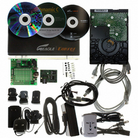
KIT APPLCTN RABBITCORE RCM4010
Manufacturer
Rabbit Semiconductor
Series
RabbitCore®r
Datasheet
1.20-101-1094.pdf
(130 pages)
Specifications of 101-1218
Main Purpose
*
Embedded
*
Utilized Ic / Part
RCM4010
Primary Attributes
*
Secondary Attributes
*
Processor To Be Evaluated
Rabbit 4000
Interface Type
Ethernet
Operating Supply Voltage
12 V
Lead Free Status / RoHS Status
Not applicable / Not applicable
Other names
316-1156


If a device such as a battery is
connected across two channels
for a differential measurement,
and it is not referenced to
analog ground, then the current
from the device will flow
through both sets of attenuator
resistors as shown in Figure 11.
This will generate a negative
voltage at one of the inputs,
LN1, which will almost cer-
tainly lead to inaccurate A/D
conversions. To make such dif-
ferential measurements, connect the R1 resistors to the A/D converter’s internal reference
voltage, which is software-configurable for 1.15 V, 2.048 V, or 2.5 V. This internal reference
voltage is available on pin 49 of header J3 as VREF, and allows you to convert analog
input voltages that are negative with respect to analog ground.
The A/D converter’s CONVERT pin is available on pin 48 of header J3 and can be used as
a hardware means of forcing the A/D converter to start a conversion cycle. The CONVERT
signal is an edge-triggered event and has a hold time of two CCLK periods for debounce.
A conversion is started by an active (rising) edge on the CONVERT pin. The CONVERT
pin must stay low for at least two CCLK periods before going high for at least two CCLK
periods. Figure 12 shows the timing of a conversion start. The double falling arrow on
CCLK indicates the actual start of the conversion cycle.
Appendix B explains the implementation examples of these features on the Prototyping
Board.
User’s Manual
NOTE: The amplifier inside the A/D converter’s internal voltage reference circuit has a
very limited output-current capability. The internal buffer can source up to 20 mA and
sink only up to 200 µA. Use a separate buffer amplifier if you need to supply any load
current.
Figure 12. Timing Diagram for Conversion Start Using CONVERT Pin
Figure 11. Current Flow from Ungrounded
I
or Floating Source
41
Related parts for 101-1218
Image
Part Number
Description
Manufacturer
Datasheet
Request
R

Part Number:
Description:
COMPUTER SNGLBD BL2120 FRCTNLOCK
Manufacturer:
Rabbit Semiconductor
Datasheet:

Part Number:
Description:
KIT MESH NETWORK ADD-ON RCM4510W
Manufacturer:
Rabbit Semiconductor
Datasheet:

Part Number:
Description:
KIT DEV FOR BL2500 COYOTE
Manufacturer:
Rabbit Semiconductor
Datasheet:

Part Number:
Description:
KIT APPLICATION SIMPLE SENSOR
Manufacturer:
Rabbit Semiconductor
Datasheet:

Part Number:
Description:
KIT ETHERNET INT'L RCM3720
Manufacturer:
Rabbit Semiconductor
Datasheet:
Part Number:
Description:
KIT SERIAL-ETHERNET APPLICATION
Manufacturer:
Rabbit Semiconductor

Part Number:
Description:
KIT APPLICATION MULTI-PORT S2E
Manufacturer:
Rabbit Semiconductor
Part Number:
Description:
KIT WEB SECURE EMBEDDED RCM3700
Manufacturer:
Rabbit Semiconductor
Datasheet:
Part Number:
Description:
MODULE RABBITCORE RCM3720
Manufacturer:
Rabbit Semiconductor
Datasheet:
Part Number:
Description:
MODULE RABBITCORE RCM3220
Manufacturer:
Rabbit Semiconductor
Datasheet:
Part Number:
Description:
MODULE RABBITCORE RCM3210
Manufacturer:
Rabbit Semiconductor
Datasheet:
Part Number:
Description:
COMPUTER SGL-BOARD OP6600 W/SRAM
Manufacturer:
Rabbit Semiconductor
Datasheet:
Part Number:
Description:
COMPUTER SGL-BD BL2000 SRAM/FLSH
Manufacturer:
Rabbit Semiconductor