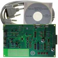
EVAL-ADE7753ZEB Analog Devices Inc, EVAL-ADE7753ZEB Datasheet
EVAL-ADE7753ZEB
Specifications of EVAL-ADE7753ZEB
Available stocks


Related parts for EVAL-ADE7753ZEB


EVAL-ADE7753ZEB Summary of contents
Page 1
FEATURES High accuracy; supports IEC 60687/61036/61268 and IEC 62053-21/62053-22/62053-23 On-chip digital integrator enables direct interface to current sensors with di/dt output A PGA in the current channel allows direct interface to shunts and current transformers Active, reactive, and apparent energy; ...
Page 2
ADE7753 TABLE OF CONTENTS Specifications ..................................................................................... 4 Timing Characteristics ..................................................................... 6 Absolute Maximum Ratings ............................................................ 7 ESD Caution .................................................................................. 7 Terminology ...................................................................................... 8 Pin Configuration and Function Descriptions ............................. 9 Typical Performance Characteristics ........................................... 11 Theory of Operation ...................................................................... 16 ...
Page 3
REVISION HISTORY 1/09—Rev Rev B Changes to Features Section ............................................................ 1 Changes to Zero-Crossing Detection Section and Period Measurement Section ..................................................................... 19 Changes to Channel 1 RMS Calculation Section, Channel 1 RMS Offset Compensation Section, and Equation 4 ...
Page 4
ADE7753 SPECIFICATIONS ± 5%, AGND = DGND = 0 V, on-chip reference, CLKIN = 3.579545 MHz XTAL the plots in the Typical Performance Characteristics section. Table 1. Parameter ENERGY MEASUREMENT ACCURACY ...
Page 5
Parameter Channel 2 Signal-to-Noise Plus Distortion Bandwidth (–3 dB) REFERENCE INPUT REF Input Voltage Range IN/OUT Input Capacitance ON-CHIP REFERENCE Reference Error Current Source Output Impedance Temperature Coefficient CLKIN Input Clock Frequency LOGIC INPUTS RESET , DIN, SCLK, CLKIN, and ...
Page 6
ADE7753 TIMING CHARACTERISTICS ± 5%, AGND = DGND = 0 V, on-chip reference, CLKIN = 3.579545 MHz XTAL Sample tested during initial release and after any redesign or process change that ...
Page 7
ABSOLUTE MAXIMUM RATINGS T = 25°C, unless otherwise noted. A Table 3. Parameter AVDD to AGND DVDD to DGND DVDD to AVDD Analog Input Voltage to AGND, V1P, V1N, V2P, and V2N Reference Input Voltage to AGND Digital Input Voltage ...
Page 8
ADE7753 TERMINOLOGY Measurement Error The error associated with the energy measurement made by the ADE7753 is defined by the following formula: = Percentage Error ⎛ − Energy Register ADE 7753 True Energy ⎜ ⎜ True Energy ⎝ Phase Error between ...
Page 9
PIN CONFIGURATION AND FUNCTION DESCRIPTIONS Table 4. Pin Function Descriptions Pin No. Mnemonic Description 1 RESET Reset Pin for the ADE7753. A logic low on this pin holds the ADCs and digital circuitry (including the serial interface reset ...
Page 10
ADE7753 Pin No. Mnemonic Description 12 ZX Voltage Waveform (Channel 2) Zero-Crossing Output. This output toggles logic high and logic low at the zero crossing of the differential signal on Channel 2—see the Zero-Crossing Detection section. 13 SAG This open-drain ...
Page 11
TYPICAL PERFORMANCE CHARACTERISTICS 0.5 GAIN = 1 0.4 INTEGRATOR OFF INTERNAL REFERENCE 0.3 –40° 0.5 0.2 0.1 +25° –0.1 +25° 0.5 –0.2 –0.3 +85° 0.5 –0.4 –0.5 0.1 1 FULL-SCALE ...
Page 12
ADE7753 0.5 GAIN = 1 0.4 INTEGRATOR OFF EXTERNAL REFERENCE 0.3 0.2 +25° 0.1 0 +25° 0.5 –0.1 –0.2 –0.3 –40° 0.5 –0.4 –0.5 0.1 1 FULL-SCALE CURRENT (%) Figure 12. Reactive Energy ...
Page 13
GAIN = 8 0.8 INTEGRATOR OFF EXTERNAL REFERENCE 0.6 0 0.2 0 –0.2 –0 0.5 –0.6 –0.8 –0 LINE FREQUENCY (Hz) Figure 18. Active Energy Error as a Percentage of Reading ...
Page 14
ADE7753 3.0 2.5 2 0.5 1.5 1.0 0 –0.5 –1.0 –1.5 –2 FREQUENCY (Hz) Figure 24. Active Energy Error as a Percentage of Reading (Gain = 8) over ...
Page 15
V DD 10μF 100nF 100nF I di/dt CURRENT AVDD DVDD RESET SENSOR DIN 100Ω 1kΩ V1P 33nF 33nF DOUT 100Ω 1kΩ SCLK V1N U1 33nF 33nF CS ADE7753 CLKOUT V2N 1kΩ 33nF CLKIN 600kΩ V2P IRQ 33nF 110V 1kΩ SAG ...
Page 16
ADE7753 THEORY OF OPERATION ANALOG INPUTS The ADE7753 has two fully differential voltage input channels. The maximum differential input voltage for input pairs V1P/V1N and V2P/V2N is ±0 addition, the maximum signal level on analog inputs for V1P/V1N ...
Page 17
DC COMPONENT (INCLUDING ERROR TERM) IS EXTRACTED BY THE LPF FOR REAL POWER CALCULATION × × × × ω 2ω 0 FREQUENCY (RAD/S) Figure 33. Effect of ...
Page 18
ADE7753 –88.0 –88.5 –89.0 –89.5 –90.0 –90 FREQUENCY (Hz) FREQ Figure 37. Combined Phase Response of the Digital Integrator and Phase Compensator –1.0 –1.5 –2.0 –2.5 –3.0 –3.5 –4.0 –4.5 –5.0 –5.5 –6 FREQUENCY ...
Page 19
The zero-crossing detection also drives the ZX flag in the interrupt status register. The ZX flag is set to Logic 0 on the rising and falling edge of the voltage waveform. It stays low until the status register is read ...
Page 20
ADE7753 CHANNEL 2 FULL SCALE SAGLVL [7:0] SAGCYC [7:0] = 0x04 3 LINE CYCLES SAG Figure 43. ADE7753 Sag Detection Figure 43 shows the line voltage falling below a threshold that is set in the sag level register (SAGLVL[7:0]) for ...
Page 21
ADE7753 INTERRUPTS ADE7753 interrupts are managed through the interrupt status register (STATUS[15:0]) and the interrupt enable register (IRQEN[15:0]). When an interrupt event occurs in the ADE7753, the corresponding flag in the status register is set to Logic 1— see the ...
Page 22
ADE7753 Interrupt Timing The ADE7753 Serial Interface section should be reviewed first before reviewing the interrupt timing. As previously described, when the IRQ output goes low, the MCU ISR must read the interrupt status register to determine the source of ...
Page 23
Antialias Filter Figure 47 also shows an analog low-pass filter (RC) on the input to the modulator. This filter is present to prevent aliasing. Aliasing is an artifact of all sampled systems. Aliasing means that frequency components in the input ...
Page 24
ADE7753 ×1, ×2, ×4, ×8, ×16 {GAIN[2:0]} V1P PGA1 V1 V1N V1 0.5V, 0.25V, 0.125V, 62.5mV, 0x2851EC 31.3mV, 15.6mV, 0V ANALOG INPUT RANGE *WHEN DIGITAL INTEGRATOR IS ENABLED, FULL-SCALE OUTPUT DATA IS ATTENUATED DEPENDING ON THE SIGNAL FREQUENCY BECAUSE THE ...
Page 25
CURRENT SIGNAL (i(t)) 0x2851EC 0x00 0xD7AE14 CHANNEL 1 With the specified full-scale analog input signal of 0.5 V, the ADC produces an output code that is approximately ±2,642,412d—see the Channel 1 ADC section. The equivalent rms value of a full-scale ...
Page 26
ADE7753 V2 ANALOG INPUT RANGE 0.5V, 0.25, 0.125, 62.5mV, 31.25mV CHANNEL 2 Channel 2 has only one analog input range (0.5 V differential). Like Channel 1, Channel 2 has a PGA with gain selections and ...
Page 27
PHASE COMPENSATION When the HPF is disabled, the phase error between Channel 1 and Channel from dc to 3.5 kHz. When HPF is enabled, Channel 1 has the phase response illustrated in Figure 58 and Figure 59. ...
Page 28
ADE7753 0.4 0.3 0.2 0.1 0.0 –0.1 –0.2 –0.3 –0 FREQUENCY (Hz) Figure 60. Combined Gain Response of the HPF and Phase Compensation ACTIVE POWER CALCULATION Power is defined as the rate of energy flow from ...
Page 29
CURRENT CHANNEL VOLTAGE CHANNEL T Figure 63 shows the signal processing chain for the active power calculation in the ADE7753. As explained, the active power is calculated by low-pass filtering the instantaneous power signal. Note that when reading the waveform ...
Page 30
ADE7753 I CURRENT SIGNAL – i(t) V VOLTAGE SIGNAL– v(t) The ADE7753 achieves the integration of the active power signal by continuously accumulating the active power signal in an internal nonreadable 49-bit energy register. The active energy register (AENERGY[23:0]) represents ...
Page 31
Integration Time under Steady Load As mentioned in the last section, the discrete time sample period (T) for the accumulation register is 1.1 μs (4/CLKIN). With full-scale sinusoidal signals on the analog inputs and the WGAIN register set to 0x000, ...
Page 32
ADE7753 The active power signal (output of LPF2) can be rewritten as ⎡ ⎤ ⎢ ⎥ ⎢ ⎥ VI ⎢ ⎥ p( − × cos(4πf 2 ⎢ ⎥ ⎛ ⎞ ⎜ ⎟ L ⎢ 1 ⎥ ...
Page 33
LINE CYCLE ENERGY ACCUMULATION MODE In line cycle energy accumulation mode, the energy accumula- tion of the ADE7753 can be synchronized to the Channel 2 zero crossing so that active energy can be accumulated over an integral number of half ...
Page 34
ADE7753 REACTIVE POWER CALCULATION Reactive power is defined as the product of the voltage and current waveforms when one of these signals is phase-shifted by 90°. The resulting waveform is called the instantaneous reactive power signal. Equation 25 gives an ...
Page 35
The features of the line reactive energy accumulation are the same as the line active energy accumulation. The number of half line cycles is specified in the LINECYC register. LINECYC is an unsigned 16-bit register. The ADE7753 can accumulate reactive ...
Page 36
ADE7753 APPARENT POWER 100% FS APPARENT POWER 150% FS APPARENT POWER 50% FS 0x103880 0xAD055 0x5682B 0x00000 0x000 0x7FF 0x800 {VAGAIN[11:0]} APPARENT POWER CALIBRATION RANGE VOLTAGE AND CURRENT CHANNEL INPUTS: 0.5V/GAIN Figure 74. Apparent Power Calculation Output Range Apparent Power ...
Page 37
Note that the apparent energy register is unsigned—see Figure 76. By using the interrupt enable register, the ADE7753 can be con- figured to issue an interrupt ( IRQ ) when the apparent energy register is more than half full or ...
Page 38
ADE7753 ENERGIES SCALING The ADE7753 provides measurements of active, reactive, and apparent energies. These measurements do not have the same scaling and thus cannot be compared directly to each other. Table 8. Energies Scaling 0.707 ...
Page 39
Watt Gain The first step of calibrating the gain is to define the line voltage, base current and the maximum current for the meter. A meter constant needs to be determined for CF, such as 3200 imp/kWh or 3.2 imp/Wh. ...
Page 40
ADE7753 The nominal sample set of meters should be measured using the default CFDEN, CFNUM, and WDIV to ensure that the best CFDEN is chosen for the design. With the CFNUM register set to 0, CFDEN is ...
Page 41
CALCULATE CFDEN VALUE FOR DESIGN WRITE CFDEN VALUE TO CFDEN REGISTER ADDR. 0x15 = CFDEN SET TEST b TEST NOM SET HALF LINECYCLES FOR ACCUMULATION IN LINECYC REGISTER ADDR. 0x1C SET MODE FOR ...
Page 42
ADE7753 With WDIV and CFNUM set to 0, LAENERGY can be expressed as LAENERGY = IB(expected) × × × INT ( CF LINECYC 2 / PERIOD IB ( expected ) IB The calculated Wh/LSB ratio for the active energy register, ...
Page 43
Calibrating Watt Offset with an Accurate Source Example Figure 83 is the flowchart for watt offset calibration with an accurate source. SET TEST MIN TEST NOM SET HALF LINE CYCLES FOR ACCUMULATION IN ...
Page 44
ADE7753 Phase Calibration The PHCAL register is provided to remove small phase errors. The ADE7753 compensates for phase error by inserting a small time delay or advance on the voltage channel input. Phase leads up to 1.84° and phase lags ...
Page 45
Calibrating Phase with an Accurate Source Example With an accurate source, line cycle accumulation is a good method of calibrating phase error. The value of LAENERGY must be obtained at two power factors and PF = 0.5 ...
Page 46
ADE7753 Voltage rms compensation is done after the square root. VRMS = VRMS0 + VRMSOS where: VRMS0 is the rms measurement without offset correction. VRMS is linear from full-scale to full-scale/20. To calibrate the offset, two VRMS measurements are required, ...
Page 47
CALCULATE CFDEN VALUE FOR DESIGN WRITE CFDEN VALUE TO CFDEN REGISTER SET I SET HALF LINE CYCLES FOR ACCUMULATION IN LINECYC REGISTER ADDR. 0x1C ACCUMULATION ADDR. 0x09 = 0x0080 ENABLE LINE CYCLE ACCUMULATION READ LINE ACCUMULATION ENERGY APPARAENT ENERGY: ADDR. ...
Page 48
ADE7753 The impulse/LSB ratio used to convert the value in the LVARENERGY register into a pulse output can be expressed in terms of impulses/VARh and VARh/LSB. × imp/LSB = imp / VARh VARh / LSB VARCF = IB(expected) × VARConstan ...
Page 49
ADE7753 SERIAL INTERFACE All ADE7753 functionality is accessible via several on-chip registers—see Figure 89. The contents of these registers can be updated or read using the on-chip serial interface. After power toggling the RESET pin low or a ...
Page 50
ADE7753 ADE7753 Serial Write Operation The serial write sequence takes place as follows. With the ADE7753 in communications mode (i.e., the CS input logic low), a write to the communications register first takes place. The MSB of this byte transfer ...
Page 51
ADE7753 Serial Read Operation During a data read operation from the ADE7753, data is shifted out at the DOUT logic output on the rising edge of SCLK the case with the data write operation, a data read must ...
Page 52
ADE7753 ADE7753 REGISTERS Table 10. Summary of Registers by Address Address Name R/W No. Bits 0x01 WAVEFORM R 24 0x02 AENERGY R 24 0x03 RAENERGY R 24 0x04 LAENERGY R 24 0x05 VAENERGY R 24 0x06 RVAENERGY R 24 0x07 ...
Page 53
Address Name R/W No. Bits 0x12 WGAIN R/W 12 0x13 WDIV R/W 8 0x14 CFNUM R/W 12 0x15 CFDEN R/W 12 0x16 IRMS R 24 0x17 VRMS R 24 0x18 IRMSOS R/W 12 0x19 VRMSOS R/W 12 0x1A VAGAIN R/W ...
Page 54
ADE7753 Address Name R/W No. Bits 0x27 PERIOD R 16 0x28– 0x3C 0x3D TMODE R/W 8 0x3E CHKSUM R 6 0x3F DIEREV Type decoder unsigned signed by twos complement method, and S 1 ...
Page 55
ADE7753 REGISTER DESCRIPTIONS All ADE7753 functionality is accessed via the on-chip registers. Each register is accessed by first writing to the communications register and then transferring the register data. A full description of the serial interface protocol is given in ...
Page 56
ADE7753 Default Bit Location Bit Mnemonic Value 14, 13 WAVSEL1 POAM 0 POAM (POSITIVE ONLY ACCUMULATION) WAVSEL (WAVEFORM SELECTION FOR SAMPLE MODE LPF2 01 = RESERVED 10 = CH1 11 = CH2 DTRT (WAVEFORM SAMPLES ...
Page 57
INTERRUPT STATUS REGISTER (0x0B), RESET INTERRUPT STATUS REGISTER (0x0C), INTERRUPT ENABLE REGISTER (0x0A) The status register is used by the MCU to determine the source of an interrupt request ( IRQ ). When an interrupt event occurs in the ADE7753, ...
Page 58
ADE7753 CH1OS REGISTER (0x0D) The CH1OS register is an 8-bit, read/write enabled register. The MSB of this register is used to switch on/off the digital integrator in Channel 1, and Bits indicates the amount of the offset ...
Page 59
... MIN COPLANARITY 0.10 ORDERING GUIDE Model Temperature Range ADE7753ARS −40°C to +85°C ADE7753ARSRL −40°C to +85°C 1 ADE7753ARSZ −40°C to +85°C 1 ADE7753ARSZRL −40°C to +85°C 1 EVAL-ADE7753ZEB RoHS Compliant Part. 7.50 7.20 6. 5.60 5.30 8.20 5.00 7.80 7. 1.85 1 ...
Page 60
ADE7753 NOTES ©2003–2009 Analog Devices, Inc. All rights reserved. Trademarks and registered trademarks are the property of their respective owners. D02875–0–1/09(B) Rev Page ...