EVAL-ADM1185EBZ Analog Devices Inc, EVAL-ADM1185EBZ Datasheet
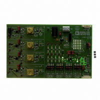
EVAL-ADM1185EBZ
Specifications of EVAL-ADM1185EBZ


Related parts for EVAL-ADM1185EBZ


EVAL-ADM1185EBZ Summary of contents
Page 1
FEATURES Powered from 2 5 the VCC pin Monitors 4 supplies via 0.8% accurate comparators Logical core with internal timeouts provides power supply sequencing and fault protection 4 inputs can be programmed to monitor different voltage ...
Page 2
ADM1185 TABLE OF CONTENTS Features .............................................................................................. 1 Applications ....................................................................................... 1 Functional Block Diagram .............................................................. 1 General Description ......................................................................... 1 Applications Diagram ...................................................................... 1 Revision History ............................................................................... 2 Specifications ..................................................................................... 3 Absolute Maximum Ratings ............................................................ 4 Thermal Resistance ...................................................................... 4 REVISION ...
Page 3
SPECIFICATIONS −40°C to +85°C, unless otherwise noted Table 1. Parameter VCC PIN Operating Voltage Range Supply Current, I VCC VIN1 TO VIN4 (VINx) PINS Input Current, I ...
Page 4
ADM1185 ABSOLUTE MAXIMUM RATINGS T = 25°C, unless otherwise noted. A Table 2. Parameter VCC Pin VINx Pins OUTx, PWRGD Pins Storage Temperature Range Operating Temperature Range Lead Temperature Soldering (10 sec) Junction Temperature Stresses above those listed under Absolute ...
Page 5
PIN CONFIGURATION AND FUNCTION DESCRIPTIONS Table 4. Pin Function Descriptions Pin No. Mnemonic Description 1 GND Chip Ground Pin. 2 VIN1 Noninverting Input of Comparator 1. The voltage on this pin is compared with a 0.6 V reference. Can be ...
Page 6
ADM1185 TYPICAL PERFORMANCE CHARACTERISTICS 0.5 1.0 1.5 2.0 2.5 3.0 SUPPLY VOLTAGE (V) Figure 4. Supply Current vs. Supply Voltage VCC = 5V 30 ...
Page 7
OVERDRIVE 2.7 2.9 3.1 3.3 3.5 3.7 3.9 4.1 4.3 4.5 4.7 VOLTAGE (V) Figure 10. VIN1 to OUT1 Falling Delay vs. Supply Voltage 50 VCC = 3.3V, 100mV OVERDRIVE 40 30 ...
Page 8
ADM1185 100 1mA SINK 100µA SINK 0 1.0 1.5 2.0 2.5 3.0 3.5 SUPPLY VOLTAGE (V) Figure 16. Output Low Voltage vs. Supply Voltage 4.0 4.5 5.0 5.5 Rev ...
Page 9
THEORY OF OPERATION The operation of the ADM1185 is explained in this section in the context of the device in a voltage monitoring and sequencing application (see Figure 18). In this application, the ADM1185 monitors four separate voltage rails, turns ...
Page 10
ADM1185 VOLTAGE MONITORING AFTER POWER-ON Once PWRGD is asserted, the logical core latches into a different mode of operation. During the initial power-up phase, each output directly depends on an input (for example, VIN3 asserting causes OUT3 to assert). When ...
Page 11
V (RISING) T VIN1 OUT1 t PROP 190ms OUT2 OUT3 PWRGD Figure 20. Power-Up Waveforms VIN1 OUT1 OUT2 OUT3 PWRGD 190ms Figure 21. Waveforms Showing Reaction to a Temporary Low Glitch OUT1 1 OUT2 2 OUT3 3 PWRGD 4 CH1 ...
Page 12
ADM1185 CASCADING MULTIPLE DEVICES Multiple ADM1185 devices can be cascaded in situations where a large number of supplies must be monitored and/or sequenced. There are numerous configurations for interconnecting devices. The most suitable configuration depends on the application. Figure 23 ...
Page 13
... OUTLINE DIMENSIONS ORDERING GUIDE Model Temperature Range 1 ADM1185ARMZ-1 −40°C to +85°C 1 ADM1185ARMZ-1REEL7 −40°C to +85°C 1 EVAL-ADM1185EBZ RoHS Compliant Part. 3.10 3.00 2. 5.15 3.10 4.90 3.00 4.65 2. PIN 1 0.50 BSC 0.95 0.85 1.10 MAX 0.75 0.15 0.33 SEATING 0.23 0.05 PLANE 0 ...
Page 14
ADM1185 NOTES Rev Page ...
Page 15
NOTES Rev Page ADM1185 ...
Page 16
ADM1185 NOTES ©2007–2009 Analog Devices, Inc. All rights reserved. Trademarks and registered trademarks are the property of their respective owners. D06196-0-6/09(B) Rev Page ...