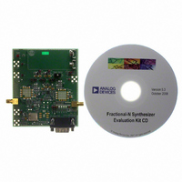
EVAL-ADF4252EBZ2 Analog Devices Inc, EVAL-ADF4252EBZ2 Datasheet
EVAL-ADF4252EBZ2
Specifications of EVAL-ADF4252EBZ2


Related parts for EVAL-ADF4252EBZ2


EVAL-ADF4252EBZ2 Summary of contents
Page 1
FEATURES 3.0 GHz Fractional-N/1.2 GHz Integer-N 2 3.3 V Power Supply Separate V Allows Extended Tuning Voltage Programmable Dual Modulus Prescaler RF: 4/5, 8/9 IF: 8/9, 16/17, 32/33, 64/65 Programmable Charge Pump Currents ...
Page 2
... MIN GHz, RF PFD = 10 MHz, MOD = 4095 500 MHz, IF PFD = 200 kHz, REF = 10 MHz The in-band phase noise is measured with the EVAL-ADF4252EB2 evaluation board and the HP5500E phase noise test system. The spectrum analyzer provides the REF for the synthesizer ( MHz @ 0 dBm). f ...
Page 3
TIMING CHARACTERISTICS Limit MIN MAX Parameter (B Version *Guaranteed by design, but not production tested. ...
Page 4
... Therefore, proper ESD precautions are recommended to avoid performance degradation or loss of functionality –0 Mode + 0 ADF4252BCP ADF4252BCP-REEL + 0 ADF4252BCP-REEL7 + 0 EVAL–ADF4252EB1 EVAL–ADF4252EB2 *CP = Chip Scale Package 2. GND –4– ORDERING GUIDE Temperature Package Range Option –40ºC to +85ºC CP-24 –40ºC to +85ºC CP-24 –40ºC to +85ºC ...
Page 5
Mnemonic Function CP RF Charge Pump Output. This is normally connected to a loop filter that drives the input to an external VCO Charge Pump Ground. GND RF A Input to the RF Prescaler. This small ...
Page 6
ADF4252 ADF4252 REF IN REF OUT HIGH Z MUXOUT CLK DATA 4-BIT R COUNTER 2 FREQUENCY DOUBLER DETECTOR V DD LOCK DETECT D GND OUTPUT MUX V ...
Page 7
... TPC plots attained using EVAL-ADF4252EB1; measurements from HP8562E spectrum analyzer 3V – 1.875mA REFERENCE CP LEVEL = – 4.2dBm PFD FREQUENCY = 10MHz –20 CHANNEL STEP = 200kHz LOOP BANDWIDTH = 20kHz FRACTION = 59/100 –30 RBW = 10Hz –40 –50 –60 –70 –80 –90 –100 –2kHz –1kHz 1.7518GHz FREQUENCY TPC 1 ...
Page 8
ADF4252 3V 1.875mA –10 REFERENCE CP PFD FREQUENCY = 20MHz LEVEL = – 4.2dBm CHANNEL STEP = 200kHz –20 LOOP BANDWIDTH = 20kHz FRACTION = 59/100 –30 RBW = 10Hz ...
Page 9
... FREQUENCY (GHz) TPC 15. 200 kHz Spur vs. Frequency* *Across all fractional channel steps from f = 0/130 129/130 1.45 GHz, Int Reg = 55, Ref = 26 MHz, and LBW = 40 kHz. Plots attained using EVAL-ADF4252EB2 evaluation board. OUT REV. B –20 –30 –40 –50 –60 – ...
Page 10
ADF4252 0 –5 –10 PRESCALER = 4/5 –15 –20 –25 –30 – FREQUENCY (GHz) TPC 19. RF Input Sensitivity ...
Page 11
CIRCUIT DESCRIPTION Reference Input Section The reference input stage is shown in Figure 3. SW1 and SW2 are normally closed switches. SW3 is normally open. When power-down is initiated, SW3 is closed and SW1 and SW2 are opened. This ensures ...
Page 12
ADF4252 Phase Frequency Detector (PFD) and Charge Pump The PFD takes inputs from the R counter and N counter and produces an output proportional to the phase and frequency difference between them. Figure simplified schematic. The antibacklash ...
Page 13
RF N DIVIDER REG 8-BIT RF INTEGER VALUE (INT) DB23 DB22 DB21 DB20 DB19 DB18 DB17 DIVIDER REG 4-BIT RF R COUNTER DB20 DB19 DB18 DIVIDER ...
Page 14
ADF4252 8-BIT RF INTEGER VALUE (INT) DB23 DB22 DB21 DB20 DB19 DB18 DB17 DB16 DB15 DB14 DB13 DB12 DB11 DB10 DB9 RESERVED 0 RESERVED ...
Page 15
RF R COUNTER DB20 DB19 DB18 DB17 DB16 DB15 REF IN DOUBLER 0 DISABLED 1 ENABLED P3 RF PRESCALER 0 4 ...
Page 16
ADF4252 RESERVED DB15 DB14 DB13 N3 T3 THESE BITS SHOULD EACH BE SET TO 0 FOR NORMAL OPERATION SETTING CP2 Table V. RF Control ...
Page 17
...
Page 18
ADF4252 IF PRESCALER* DB19 DB18 DB17 DB23 DB22 DB21 DB20 P15 P14 P13 B12 B11 B10 B9 P14 P13 PRESCALER VALUE 16/ 32/ 64/65 P15 IF CP GAIN 0 DISABLED 1 ...
Page 19
DB18 DB17 DB16 DB15 DB14 R14 P16 R15 R13 R12 R15 32764 32765 32766 32767 P16 IF REF IN DOUBLER 0 DISABLED 1 ENABLED REV. B Table VIII Divider Register Map ...
Page 20
ADF4252 RF PHASE RESERVED RESYNC DB15 DB14 DB13 PR3 PR2 T8 THESE BITS SHOULD BE SET TO 0 FOR NORMAL OPERATION PR3 PR2 PR1 CP3 IF CP2 IF CP1 ...
Page 21
RF N DIVIDER REGISTER (Address R0) With R0[ set to [0, 0, 0], the on-chip RF N divider register will be programmed. Table III shows the input data format for programming this register. 8-Bit RF INT Value These ...
Page 22
ADF4252 RF Phase Detector Polarity DB7 in the ADF4252 sets the RF phase detector polarity. When the VCO characteristics are positive, this should be set to 1. When they are negative, it should be set Charge Pump ...
Page 23
IF Counter Reset DB3 is the IF counter reset bit for the ADF4252. When this is 1, the IF synthesizer counters are held in reset. For normal operation, this bit should Charge Pump Three-State This bit puts ...
Page 24
ADF4252 So, from Equation × MHz PFD 1 = × GHz 13 MHz INT + where INT = 138 and FRAC = 30. IF Synthesizer: An Example ...
Page 25
RF carrier. Harmonics of all spurs mentioned will also appear. With the lowest spur setting enabled, the spurs will be attenuated into the noise floor. Prescaler The prescaler limits the INT value. With P = ...
Page 26
ADF4252 VVCO R48 0 6.3V 6. OUT C10 C4 J6 10pF 10pF C15 100pF 14 R12 VCC R17 18 13k OUT R13 C16 C20 18 100pF VCO2 82pF ...
Page 27
PIN 1 INDICATOR 1.00 0.85 0.80 SEATING PLANE REV. B OUTLINE DIMENSIONS 24-Lead Lead Frame Chip Scale Package [LFCSP] (CP-24) Dimensions shown in millimeters 4.0 BSC SQ 0.60 MAX 0.50 BSC 3.75 TOP BSC SQ VIEW 0.50 0.40 0.30 0.80 ...
Page 28
ADF4252 Revision History Location 10/03—Data Sheet changed from REV REV. B. Change to SPECIFICATIONS . . . . . . . . . . . . . . . . . . . . . . . . ...