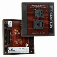
AC164336 Microchip Technology, AC164336 Datasheet - Page 190
AC164336
Manufacturer Part Number
AC164336
Description
MODULE SOCKET FOR PM3 28/44QFN
Manufacturer
Microchip Technology
Datasheet
1.AC164335.pdf
(286 pages)
Specifications of AC164336
Module/board Type
Socket Module - QFN
Product
Microcontroller Accessories
Lead Free Status / RoHS Status
Not applicable / Not applicable
For Use With/related Products
MPLAB® PM3
Lead Free Status / RoHS Status
Lead free / RoHS Compliant, Not applicable / Not applicable


dsPIC30F1010/202X
16.18 Module Power-Down Modes
The module has two internal power modes.
When the ADON bit is ‘1’, the module is in Active mode
and is fully powered and functional.
When ADON is ‘0’, the module is in Off mode. The state
machine for the module is reset, as are all of the
pending conversion requests.
To return to the Active mode from Off mode, the user
must wait for the bias generators to stabilize. The
stabilization time is specified in the electrical specs.
16.19 Effects of a Reset
A device Reset forces all registers to their Reset state.
This forces the ADC module to be turned off, and any
conversion and sampling sequence is aborted. The
value that is in the ADCBUFx register is not modified.
The ADCBUFx registers contain unknown data after a
Power-on Reset.
DS70178C-page 188
Preliminary
16.20 Configuring Analog Port Pins
The use of the ADPCFG and TRIS registers control the
operation of the A/D port pins.
The port pins that are desired as analog inputs should
have their corresponding TRIS bit set (input). If the
TRIS bit is cleared (output), the digital output level (V
or V
Port pins that are desired as analog inputs must have
the corresponding ADPCFG bit clear. This will config-
ure the port to disable the digital input buffer. Analog
levels on pins where ADPCFG<n> = 1, may cause the
digital input buffer to consume excessive current.
If a pin is not configured as an analog input
ADPCFG<n> = 1, the analog input is forced to AVss,
and conversions of that input do not yield meaningful
results.
When reading the PORT register, all pins configured as
analog input ADPCFG<n> = 0 will read ‘0’.
The A/D operation is independent of the state of the
input selection bits and the TRIS bits.
16.21 Output Formats
The A/D converts 10 bits. The data buffer RAM is 16
bits wide. The ADC data can be read in one of two dif-
ferent formats, as shown in Figure 16-5. The FORM bit
selects the format. Each of the output formats
translates to a 16-bit result on the data bus.
OL
) will be converted.
© 2006 Microchip Technology Inc.
OH
Related parts for AC164336
Image
Part Number
Description
Manufacturer
Datasheet
Request
R

Part Number:
Description:
Manufacturer:
Microchip Technology Inc.
Datasheet:
Part Number:
Description:
Manufacturer:
Microchip Technology Inc.
Datasheet:
Part Number:
Description:
Manufacturer:
Microchip Technology Inc.
Datasheet:
Part Number:
Description:
Manufacturer:
Microchip Technology Inc.
Datasheet:
Part Number:
Description:
Manufacturer:
Microchip Technology Inc.
Datasheet:
Part Number:
Description:
Manufacturer:
Microchip Technology Inc.
Datasheet:
Part Number:
Description:
Manufacturer:
Microchip Technology Inc.
Datasheet:
Part Number:
Description:
Manufacturer:
Microchip Technology Inc.
Datasheet: