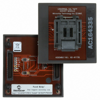
AC164335 Microchip Technology, AC164335 Datasheet - Page 84
AC164335
Manufacturer Part Number
AC164335
Description
MODULE SKT FOR 10X10 PM3 44TQFP
Manufacturer
Microchip Technology
Datasheet
1.AC164335.pdf
(286 pages)
Specifications of AC164335
Module/board Type
Socket Module - TQFP
Product
Microcontroller Accessories
Lead Free Status / RoHS Status
Not applicable / Not applicable
For Use With/related Products
MPLAB® PM3
For Use With
DV007003 - PROGRAMMER UNIVERSAL PROMATE II
Lead Free Status / RoHS Status
Lead free / RoHS Compliant, Not applicable / Not applicable


dsPIC30F1010/202X
7.4
The dsPIC30F Flash program memory is organized
into rows and panels. Each row consists of 32 instruc-
tions, or 96 bytes. Each panel consists of 128 rows, or
4K x 24 instructions. RTSP allows the user to erase one
row (32 instructions) at a time and to program 32
instructions at one time. RTSP may be used to program
multiple program memory panels, but the table pointer
must be changed at each panel boundary.
Each panel of program memory contains write latches
that hold 32 instructions of programming data. Prior to
the actual programming operation, the write data must
be loaded into the panel write latches. The data to be
programmed into the panel is loaded in sequential
order into the write latches; instruction ‘0’, instruction
‘1’, etc. The instruction words loaded must always be
from a group of 32 boundary.
The basic sequence for RTSP programming is to set up
a table pointer, then do a series of TBLWT instructions
to load the write latches. Programming is performed by
setting the special bits in the NVMCON register. 32
TBLWTL and four TBLWTH instructions are required to
load the 32 instructions. If multiple panel programming
is required, the table pointer needs to be changed and
the next set of multiple write latches written.
All of the table write operations are single-word writes
(2 instruction cycles), because only the table latches
are written. A programming cycle is required for
programming each row.
The Flash Program Memory is readable, writable and
erasable during normal operation over the entire V
range.
DS70178C-page 82
RTSP Operation
Preliminary
DD
7.5
The four SFRs used to read and write the program
Flash memory are:
• NVMCON
• NVMADR
• NVMADRU
• NVMKEY
7.5.1
The NVMCON register controls which blocks are to be
erased, which memory type is to be programmed and
the start of the programming cycle.
7.5.2
The NVMADR register is used to hold the lower two
bytes of the effective address. The NVMADR register
captures the EA<15:0> of the last table instruction that
has been executed and selects the row to write.
7.5.3
The NVMADRU register is used to hold the upper byte
of the effective address. The NVMADRU register cap-
tures the EA<23:16> of the last table instruction that
has been executed.
7.5.4
NVMKEY is a write-only register that is used for write
protection. To start a programming or an erase
sequence, the user must consecutively write 0x55 and
0xAA to the NVMKEY register. Refer to Section 7.6
“Programming Operations” for further details.
Note:
Control Registers
NVMCON REGISTER
NVMADR REGISTER
NVMADRU REGISTER
NVMKEY REGISTER
The user can also directly write to the
NVMADR and NVMADRU registers to
specify a program memory address for
erasing or programming.
© 2006 Microchip Technology Inc.
Related parts for AC164335
Image
Part Number
Description
Manufacturer
Datasheet
Request
R

Part Number:
Description:
Manufacturer:
Microchip Technology Inc.
Datasheet:
Part Number:
Description:
Manufacturer:
Microchip Technology Inc.
Datasheet:
Part Number:
Description:
Manufacturer:
Microchip Technology Inc.
Datasheet:
Part Number:
Description:
Manufacturer:
Microchip Technology Inc.
Datasheet:
Part Number:
Description:
Manufacturer:
Microchip Technology Inc.
Datasheet:
Part Number:
Description:
Manufacturer:
Microchip Technology Inc.
Datasheet:
Part Number:
Description:
Manufacturer:
Microchip Technology Inc.
Datasheet:
Part Number:
Description:
Manufacturer:
Microchip Technology Inc.
Datasheet: