HW-FLYLEADS Xilinx Inc, HW-FLYLEADS Datasheet - Page 13
HW-FLYLEADS
Manufacturer Part Number
HW-FLYLEADS
Description
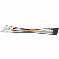
LEAD WIRES FLYING CABLE III/IV
Manufacturer
Xilinx Inc
Datasheet
1.HW-FLYLEADS.pdf
(20 pages)
Specifications of HW-FLYLEADS
Accessory Type
Parallel Cable
For Use With/related Products
Xilinx FPGA, CPLDS, Platform Flash PROMs, XC18V00 PROMs, System ACE MPM
Lead Free Status / RoHS Status
Contains lead / RoHS non-compliant
Other names
122-1473
Available stocks
Company
Part Number
Manufacturer
Quantity
Price


Signal Integrity
Platform Cable USB uses high-slew-rate buffers to drive
TCK_CCLK_SCK, TMS_PROG_SS, and TDI_DIN_MOSI.
Each buffer has a 30Ω series termination resistor. Users
should pay close attention to PCB layout to avoid
transmission line effects. Visit the Xilinx
Central
XAPP361, Planning for High Speed XC9500XV Designs, for
detailed signal integrity assistance.
If the target system has only one programmable device, the
2 mm connector should be located as close as possible to
the target device. If there are multiple devices in a single
chain on the target system, users should consider buffering
TCK_CCLK_SCK. Differential driver/receiver pairs provide
excellent signal quality when the rules identified in
Figure 25
devices are distributed over a large PCB area.
Each differential driver and/or receiver pair contributes
approximately 5 ns of propagation delay. This is
insignificant when using 12 MHz or slower clock speeds.
Each differential receiver can drive multiple target devices if
there are no branches on the PCB trace and the total trace
Target System Connections
Multiple devices can be cascaded when using either JTAG
or slave-serial topology in target systems.
page 14
page 14
The Platform Cable USB can connect directly to a single
SPI flash device.
connections. Refer to XAPP951, Configuring Xilinx FPGAs
with SPI Serial Flash, for a detailed reference design
showing the cable connections for programming an FPGA
bitstream into a SPI flash device.
The DONE pin on FPGAs can be programmed to be an
open-drain or active driver. For cascaded slave-serial
topologies, an external pull-up resistor should be used, and
all devices should be programmed for open-drain operation.
If the 2 mm connector is located a significant distance from
the target device, it is best to buffer TCK_CCLK_SCK, at a
minimum. These diagrams are intended to represent the
logical relationship between Platform Cable USB and target
devices. Refer to
buffering and termination information.
DS300 (v3.2) May 14, 2008
Product Specification
website, and see specifically Xilinx Application Note
shows typical JTAG connections, and
shows an example of slave-serial routing.
are followed. Buffering is essential if target
R
Figure 26
"Signal Integrity," page 13
shows example SPI flash
Signal Integrity
Figure 27,
for additional
Figure 28,
www.xilinx.com
length is less than four inches. A series termination resistor
should be placed adjacent to the single-ended output of the
differential receiver.
X-Ref Target - Figure 25
Note:
TCK_CCLK_SCK and the 24 MHz clock rate is used, it is
recommended that the same buffer type also be provided for
TMS_PROG_SS. This maintains a consistent phase relationship
between TCK_CCLK_SCK and TMS_PROG_SS. A buffer is not
needed for TDI_DIN_MOSI, because it sees only one load.
X-Ref Target - Figure 26
TCK_CCLK
Notes:
1. The example shows pin names for an STMicrosystems M25Pxx serial flash
2. Attach the following 2 mm connector pins to digital ground: 1, 3, 5, 7, 9, 11, 13.
3. Typically, an FPGA and other slave SPI devices, which are not shown, are
GND
MISO
MOSI
device. SPI flash devices from other vendors can have different pin names and
requirements. See the SPI flash data sheet for the equivalent pins and device
requirements.
connected to the SPI bus. The other devices on the SPI bus must be disabled
when the cable is connected to the 2 mm connector to avoid signal contention.
When a Xilinx FPGA is connected to the SPI bus, the FPGA PROG_B pin can
be held Low to ensure the FPGA pins are kept in a high-impedance state.
V
SCK
REF
SS
Figure 25: Differential Clock Buffer Example
(2)
If the target system incorporates a buffer for
Connector
2 mm
Four Differential
SN65LVDS105
10
X
2
8
4
6
Figure 26: Example of SPI Topology
Drivers
+3.3V
1
4
SPI Bus
Locate driver package adjacent to 2mm connector
SN65LVDS2 (2)
(3)
Route A & B traces for each differential
pair in parallel with equal length and
consistent spacing
D
Q
S
C
Locate one receiver adacent
to each target device
Serial Flash
M25Pxx
ST Micro
+3.3V
GND
VCC
TCK_CCLK_1
TCK_CCLK_4
Series Termination Resistor
Platform Cable USB
(1)
HOLD
W
DS300_24_110804
DS300_30_021607
Four
Buffered
Clocks
‘1’
‘1’
13
Related parts for HW-FLYLEADS
Image
Part Number
Description
Manufacturer
Datasheet
Request
R

Part Number:
Description:
BOARD ADAPTER AND FLY LEADS
Manufacturer:
Xilinx Inc
Datasheet:

Part Number:
Description:
CONN HEADER .25" VERT 4POS T/H
Manufacturer:
Samtec Inc
Part Number:
Description:
CONN HEADER .25" VERT 4POS SMD
Manufacturer:
Samtec Inc
Part Number:
Description:
CONN HEADER .25" VERT 10POS SMD
Manufacturer:
Samtec Inc
Part Number:
Description:
Conn Board Stacker HDR 28 POS 2.54mm Solder ST SMD
Manufacturer:
Samtec Inc
Datasheet:
Part Number:
Description:
CONN BOARD STACK 28POS SMD
Manufacturer:
Samtec Inc
Datasheet:

Part Number:
Description:
IC CPLD .8K 36MCELL 44-VQFP
Manufacturer:
Xilinx Inc
Datasheet:

Part Number:
Description:
IC CPLD 72MCRCELL 10NS 44VQFP
Manufacturer:
Xilinx Inc
Datasheet:

Part Number:
Description:
IC CPLD 1.6K 72MCELL 64-VQFP
Manufacturer:
Xilinx Inc
Datasheet:

Part Number:
Description:
IC CR-II CPLD 64MCELL 44-VQFP
Manufacturer:
Xilinx Inc
Datasheet:

Part Number:
Description:
IC CPLD 1.6K 72MCELL 100-TQFP
Manufacturer:
Xilinx Inc
Datasheet:

Part Number:
Description:
IC CR-II CPLD 64MCELL 56-BGA
Manufacturer:
Xilinx Inc
Datasheet: