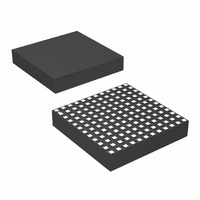
LTM4615IV#PBF Linear Technology, LTM4615IV#PBF Datasheet - Page 13

LTM4615IV#PBF
Manufacturer Part Number
LTM4615IV#PBF
Description
IC SWIT REG BUCK 4A ADJ 144LGA
Manufacturer
Linear Technology
Series
µModuler
Type
Point of Load (POL) Non-Isolatedr
Specifications of LTM4615IV#PBF
Design Resources
LTM4615 Spice Model
Output
0.8 ~ 5 V
Number Of Outputs
3
Power (watts)
12W
Mounting Type
Surface Mount
Voltage - Input
2.38 ~ 5.5 V
Package / Case
144-LGA
1st Output
0.8 ~ 5 VDC @ 4A
2nd Output
0.8 ~ 5 VDC @ 4A
3rd Output
0.8 ~ 5 VDC @ 4A
Size / Dimension
0.59" L x 0.59" W x 0.11" H (15mm x 15mm x 2.8mm)
Power (watts) - Rated
12W
Operating Temperature
-40°C ~ 125°C
Efficiency
95%
Primary Input Voltage
5.5V
No. Of Outputs
3
Output Voltage
5V
Output Current
1.5A
Voltage Regulator Case Style
LGA
No. Of Pins
144
Operating Temperature Range
-40°C To +125°C
Rohs Compliant
Yes
Dc To Dc Converter Type
Step Down
Pin Count
144
Input Voltage
5.5V
Switching Freq
1250KHz
Package Type
LGA
Output Type
Adjustable
Switching Regulator
Yes
Mounting
Surface Mount
Input Voltage (min)
2.375V
Operating Temperature Classification
Automotive
Lead Free Status / RoHS Status
Lead free / RoHS Compliant
Available stocks
Company
Part Number
Manufacturer
Quantity
Price
APPLICATIONS INFORMATION
TRACK1 is the track ramp applied to the slave’s track pin.
TRACK1 applies the track reference for the slave output up
to the point of the programmed value at which TRACK1
proceeds beyond the 0.8V reference value. The TRACK1
pin must go beyond the 0.8V to ensure the slave output
has reached its fi nal value.
Ratiometric tracking can be achieved by a few simple
calculations and the slew rate value applied to the master’s
TRACK pin. As mentioned above, the TRACK pin has a
control range from 0V to 0.8V. The control ramp slew rate
applied to the master’s TRACK pin is directly equal to the
master’s output slew rate in Volts/Time.
The equation:
where MR is the master’s output slew rate and SR is the
slave’s output slew rate in Volts/Time. When coincident
tracking is desired, then MR and SR are equal, thus R
is equal to 4.99k. R
where V
tor, and V
feedback resistor of the slave regulator in equal slew rate
or coincident tracking, then R
V
TRACK
R
MR
SR
TA
. Therefore R
• . 4 99 =
=
FB
Figure 3. Output Voltage Coincident Tracking
TRACK
4 99
is the feedback voltage reference of the regula-
V
.
FB
k R
k
is 0.8V. Since R
+
R
TB
TA
0 8
V
TB
.
FB
FB
is derived from equation:
= 4.99k and R
V
–
V
TIME
TRACK
R
TB
TA
TB
is equal to R
MASTER OUTPUT
is equal to the 4.99k top
SLAVE OUTPUT
TA
= 10k in Figure 2.
4615 F03
FB
with V
FB
TB
=
Figure 3 shows the output voltage tracking waveform for
coincident tracking.
In ratiometric tracking, a different slew rate maybe desired
for the slave regulator. R
slower than MR. Make sure that the slave supply slew rate
is chosen to be fast enough so that the slave output voltage
will reach it fi nal value before the master output.
For example, MR = 2.5V/ms and SR = 1.8V/1ms. Then
R
output must be greater than the slave output for the
tracking to work. Output load current must be present
for tracking to operate properly during power-down.
Power Good
PGOOD1 and PGOOD2 are open-drain pins that can be
used to monitor valid output voltage regulation. These pins
monitor a ±7.5% window around the regulation point.
COMP Pin
This pin is the external compensation pin. The module has
already been internally compensated for all output voltages.
Table 4 is provided for most application requirements. The
Linear Technology μModule Power Design Tool will be
provided for other control loop optimization. The COMP
pins must be tied together in parallel operation.
Parallel Switching Regulator Operation
The LTM4615 switching regulators are inherently current
mode control. Paralleling will have very good current
sharing. This will balance the thermals on the design.
Figure 13 shows a schematic of a parallel design. The
voltage feedback equation changes with the variable N
as channels are paralleled.
The equation:
N is the number of paralleled channels.
TB
V
= 6.98k. Solve for R
OUT
=
0 8
.
V
•
4 99
.
N
R
k
FB
TA
TB
+
to equal to 3.24k. The master
R
can be solved for when SR is
FB
LTM4615
13
4615f


