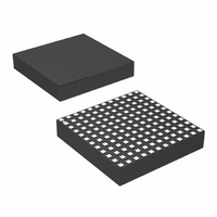
LTM4615IV#PBF Linear Technology, LTM4615IV#PBF Datasheet - Page 10

LTM4615IV#PBF
Manufacturer Part Number
LTM4615IV#PBF
Description
IC SWIT REG BUCK 4A ADJ 144LGA
Manufacturer
Linear Technology
Series
µModuler
Type
Point of Load (POL) Non-Isolatedr
Specifications of LTM4615IV#PBF
Design Resources
LTM4615 Spice Model
Output
0.8 ~ 5 V
Number Of Outputs
3
Power (watts)
12W
Mounting Type
Surface Mount
Voltage - Input
2.38 ~ 5.5 V
Package / Case
144-LGA
1st Output
0.8 ~ 5 VDC @ 4A
2nd Output
0.8 ~ 5 VDC @ 4A
3rd Output
0.8 ~ 5 VDC @ 4A
Size / Dimension
0.59" L x 0.59" W x 0.11" H (15mm x 15mm x 2.8mm)
Power (watts) - Rated
12W
Operating Temperature
-40°C ~ 125°C
Efficiency
95%
Primary Input Voltage
5.5V
No. Of Outputs
3
Output Voltage
5V
Output Current
1.5A
Voltage Regulator Case Style
LGA
No. Of Pins
144
Operating Temperature Range
-40°C To +125°C
Rohs Compliant
Yes
Dc To Dc Converter Type
Step Down
Pin Count
144
Input Voltage
5.5V
Switching Freq
1250KHz
Package Type
LGA
Output Type
Adjustable
Switching Regulator
Yes
Mounting
Surface Mount
Input Voltage (min)
2.375V
Operating Temperature Classification
Automotive
Lead Free Status / RoHS Status
Lead free / RoHS Compliant
Available stocks
Company
Part Number
Manufacturer
Quantity
Price
OPERATION
LTM4615
LTM4615 POWER MODULE DESCRIPTION
Dual Switching Regulator Section
The LTM4615 is a standalone dual nonisolated switching
mode DC/DC power supply with an additional onboard 1.5A
VLDO. It can deliver up to 4A of DC output current for each
channel with few external input and output capacitors. This
module provides two precisely regulated output voltages
programmable via one external resistor for each channel
from 0.8V DC to 5V DC over a 2.375V to 5.5V input voltage.
The VLDO is an independent 1.5A linear regulator that can
be powered from either switching converter. The typical
application schematic is shown in Figure 12.
The LTM4615 has two integrated constant frequency cur-
rent mode regulators, with built-in power MOSFETs with
fast switching speed. The typical switching frequency is
1.25MHz. With current mode control and internal feedback
loop compensation, these switching regulators have suf-
fi cient stability margins and good transient performance
under a wide range of operating conditions, and with a
wide range of output capacitors, even all ceramic output
capacitors.
Current mode control provides cycle-by-cycle fast current
limit. Besides, current limiting is provided in an overcurrent
condition with thermal shutdown. In addition, internal
overvoltage and undervoltage comparators pull the open-
drain PGOOD outputs low if the particular output feedback
voltage exits a ±7.5% window around the regulation point.
Furthermore, in an overvoltage condition, internal top FET,
M1, is turned off and bottom FET, M2, is turned on and
held on until the overvoltage condition clears, or current
limit is exceeded.
Pulling each specifi c RUN pin below 0.8V forces the spe-
cifi c regulator controller into its shutdown state, turning
off both M1 and M2 for each power stage. At low load
current, each regulator works in continuous current mode
by default to achieve minimum output voltage ripple.
The TRACK/SS pins are used for power supply tracking
and soft-start programming for each specifi c regulator.
See the Applications Information section.
10
The LTM4615 is internally compensated to be stable over
the operating conditions. Table 4 provides a guideline for
input and output capacitance for several operating condi-
tions. The Linear Technology μModule Power Design Tool
will be provided for transient and stability analysis.
The FB pins are used to program the specifi c output volt-
age with a single resistor to ground.
VLDO Section
The VLDO (very low dropout) linear regulator operates
from a 1.14V to 3.5V input. The VLDO uses an internal
NMOS transistor as the pass device in a source-follower
confi guration. The BOOST3 pin is the output of an inter-
nal boost converter that supplies the higher supply drive
to the pass device for low dropout enhancement. The
internal boost converter operates on very low current,
thus optimizing high effi ciency for the VLDO in close to
dropout operation.
An undervoltage lockout comparator on the LDO ensures
that the boost voltage is greater than 4.2V before enabling
the LDO, otherwise the LDO is disabled.
The LDO provides a high accuracy output capable of supply
1.5A of output current with a typical drop out of 100mV.
A single ceramic 10μF capacitor is all that is required
for output capacitor bypassing. A low reference voltage
allows the VLDO to have lower output voltages than the
commonly available LDO.
The device also includes current limit and thermal over-
load protection. The NMOS follower architecture has fast
transient response without the traditional high drive cur-
rents in dropout. The VLDO includes a soft-start feature
to prevent excessive current on the input during start-up.
When the VLDO is enabled, the soft-start circuitry gradu-
ally increases the 0.4V reference voltage over a period of
approximately 200μs.
4615f


