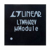
LTM4602EV#PBF Linear Technology, LTM4602EV#PBF Datasheet - Page 9

LTM4602EV#PBF
Manufacturer Part Number
LTM4602EV#PBF
Description
IC DC/DC UMODULE 6A 104-LGA
Manufacturer
Linear Technology
Series
µModuler
Type
Point of Load (POL) Non-Isolatedr
Datasheet
1.LTM4602EVPBF.pdf
(24 pages)
Specifications of LTM4602EV#PBF
Design Resources
LTM4602 Spice Model
Output
0.6 ~ 5 V
Number Of Outputs
1
Power (watts)
30W
Mounting Type
Surface Mount
Voltage - Input
4.5 ~ 20V
Package / Case
104-LGA
1st Output
0.6 ~ 5 VDC @ 6A
Size / Dimension
0.59" L x 0.59" W x 0.11" H (15mm x 15mm x 2.8mm)
Power (watts) - Rated
30W
Operating Temperature
-40°C ~ 85°C
Efficiency
92%
Lead Free Status / RoHS Status
Lead free / RoHS Compliant
3rd Output
-
2nd Output
-
Available stocks
Company
Part Number
Manufacturer
Quantity
Price
APPLICATIONS INFORMATION
The typical LTM4602 application circuit is shown in Fig-
ure 21. External component selection is primarily deter-
mined by the maximum load current and output voltage.
Output Voltage Programming and Margining
The PWM controller of the LTM4602 has an internal
0.6V reference voltage. As shown in the block diagram,
a 100k/0.5% internal feedback resistor connects V
and V
SGND pin programs the output voltage:
Table 1 shows the standard values of 1% R
for typical output voltages:
Table 1
Voltage margining is the dynamic adjustment of the output
voltage to its worst case operating range in production
testing to stress the load circuitry, verify control/protec-
tion functionality of the board and improve the system
reliability. Figure 2 shows how to implement margining
function with the LTM4602. In addition to the feedback
resistor R
Turn off both transistor Q
margining. When Q
voltage is margined up. The output voltage is margined
down when Q
R
(kΩ)
V
(V)
OUT
SET
V
OUT
OSET
Open
0.6
Figure 2. LTM4602 Margining Implementation
LTM4602
= 0.6V •
PGND
SET
pins. Adding a resistor R
, several external components are added.
100
1.2
DOWN
100k + R
UP
66.5
100k
1.5
is on and Q
R
SGND
is on and Q
SET
SET
49.9
UP
1.8
V
V
OUT
OSET
and Q
43.2
UP
2
DOWN
R
SET
SET
DOWN
is off. If the output
from V
31.6
2.5
is off, the output
R
R
DOWN
2N7002
UP
2N7002
to disable the
4602 F02
SET
Q
Q
22.1
OSET
3.3
DOWN
UP
resistor
pin to
13.7
OUT
5
voltage V
the resistor values of R
from the following equations:
Input Capacitors
The LTM4602 μModule should be connected to a low
AC-impedance DC source. High frequency, low ESR input
capacitors are required to be placed adjacent to the mod-
ule. In Figure 21, the bulk input capacitor C
for its ability to handle the large RMS current into the
converter. For a buck converter, the switching duty cycle
can be estimated as:
Without considering the inductor current ripple, the RMS
current of the input capacitor can be estimated as:
In the above equation, η% is the estimated effi ciency of
the power module. C1 can be a switcher-rated electrolytic
aluminum capacitor, OS-CON capacitor or high volume
ceramic capacitors. Note the capacitor ripple current
ratings are often based on only 2000 hours of life. This
makes it advisable to properly derate the input capacitor,
or choose a capacitor rated at a higher temperature than
required. Always contact the capacitor manufacturer for
derating requirements.
In Figure 21, the input capacitors are used as high frequency
input decoupling capacitors. In a typical 6A output applica-
tion, 1-2 pieces of very low ESR X5R or X7R, 10μF ceramic
capacitors are recommended. This decoupling capacitor
should be placed directly adjacent the module input pins
in the PCB layout to minimize the trace inductance and
high frequency AC noise.
I
D =
(R
R
CIN(RMS)
R
SET
SET
SET
(R
V
V
OUT
+ (100k
IN
OUT
SET
• V
R
UP
OUT
=
needs to be margined up/down by ±M%,
R
) • V
I
OUT(MAX)
UP
• (1– M%)
OUT
) + 100k
%
R
DOWN
• (1+ M%)
UP
• D • (1 D)
and R
)
= 0.6V
DOWN
= 0.6V
LTM4602
can be calculated
IN
is selected
4602fa
9


