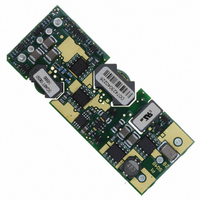
SQ48T10050-NBB0 POWER ONE, SQ48T10050-NBB0 Datasheet - Page 6

SQ48T10050-NBB0
Manufacturer Part Number
SQ48T10050-NBB0
Description
CONV DC-DC 48V IN 5V OUT 50W
Manufacturer
POWER ONE
Series
SQ48r
Type
Isolatedr
Datasheet
1.SQ48T15018-NBB0.pdf
(64 pages)
Specifications of SQ48T10050-NBB0
Output
5V
Number Of Outputs
1
Power (watts)
50W
Mounting Type
Through Hole
Voltage - Input
36 ~ 75V
Package / Case
8-DIP Module, 1/4 Brick
1st Output
5 VDC @ 10A
Size / Dimension
2.30" L x 0.90" W x 0.34" H (58.4mm x 22.9mm x 8.6mm)
Power (watts) - Rated
50W
Operating Temperature
-40°C ~ 85°C
Approvals
cUL, EN, UL
Lead Free Status / RoHS Status
Contains lead / RoHS non-compliant
3rd Output
-
2nd Output
-
4th Output
-
Other names
179-2212
SQ48T10050-NAA0
SQ48T10050-NBBO
SQ48T10050-NAA0
SQ48T10050-NBBO
Available stocks
Company
Part Number
Manufacturer
Quantity
Price
Part Number:
SQ48T10050-NBB0G
Manufacturer:
POWER-ONE
Quantity:
20 000
Test Conditions
All data presented were taken with the converter
soldered to a test board, specifically a 0.060” thick
printed wiring board (PWB) with four layers. The top
and bottom layers were not metalized. The two inner
layers, comprised of two-ounce copper, were used to
provide traces for connectivity to the converter.
The lack of metalization on the outer layers as well
as the limited thermal connection ensured that heat
transfer from the converter to the PWB was
minimized. This provides a worst-case but consistent
scenario for thermal derating purposes.
All measurements requiring airflow were made in the
vertical and horizontal wind tunnel using Infrared (IR)
thermography and thermocouples for thermometry.
Ensuring components on the converter do not
exceed their ratings is important to maintaining high
reliability. If one anticipates operating the converter
at or close to the maximum loads specified in the
derating curves, it is prudent to check actual
operating
Thermographic imaging is preferable; if this capability
is not available, then thermocouples may be used.
The use of AWG #40 gauge thermocouples is
recommended to ensure measurement accuracy.
Careful routing of the thermocouple leads will further
minimize measurement error. Refer to Fig. E for the
optimum measuring thermocouple location.
Thermal Derating
Load current vs. ambient temperature and airflow
rates are given in Fig. x.1 to Fig. x.4 for through-hole
and surface-mount versions. Ambient temperature
was varied between 25 °C and 85 °C, with airflow
rates from 30 to 500 LFM (0.15 to 2.5 m/s), and
vertical and horizontal converter mounting.
For each set of conditions, the maximum load current
was defined as the lowest of:
(i) The output current at which any FET junction
temperature does not exceed a maximum specified
temperature
thermographic image, or
SEP 14, 2005 revised to NOV 06, 2006
Fig. E: Location of the thermocouple for thermal testing.
temperatures
(120°C)
as
in
indicated
the
application.
by
the
Page 6 of 64
36-75 VDC Input; 1.0-12 VDC Output
(ii) The nominal rating of the converter (4 A on 12 V,
5.3 A on 8.0 V, 8 A on 6.0 V, 10 A on 5.0 V, and 15 A
on 3.3 – 1.0 V)).
During normal operation, derating curves
maximum FET temperature less or equal to 120 °C
should not be exceeded. Temperature on the PCB at
thermocouple location shown in Fig. E should not
exceed 118 °C in order to operate inside the derating
curves.
Efficiency
Fig. x.5 shows the efficiency vs. load current plot for
ambient temperature of 25 ºC, airflow rate of 300 LFM
(1.5 m/s) with vertical mounting and input voltages of
36 V, 48 V and 72 V. Also, a plot of efficiency vs. load
current, as a function of ambient temperature with
Vin = 48 V, airflow rate of 200 LFM (1 m/s) with
vertical mounting is shown in Fig. x.6.
Power Dissipation
Fig. x.7 shows the power dissipation vs. load current
plot for Ta = 25 ºC, airflow rate of 300 LFM (1.5 m/s)
with vertical mounting and input voltages of 36 V, 48
V and 72 V. Also, a plot of power dissipation vs. load
current, as a function of ambient temperature with
Vin = 48 V, airflow rate of 200 LFM (1 m/s) with
vertical mounting is shown in Fig. x.8.
Startup
Output
transient using the ON/OFF pin for full rated load
currents (resistive load) are shown without and with
external load capacitance in Fig. x.9 and Fig. x.10,
respectively.
Ripple and Noise
Fig. x.13 shows the output voltage ripple waveform,
measured at full rated load current with a 10 µF
tantalum and 1 µF ceramic capacitor across the
output. Note that all output voltage waveforms are
measured across a 1 µF ceramic capacitor.
The input reflected ripple current waveforms are
obtained using the test setup shown in Fig x.14. The
corresponding waveforms are shown in Fig. x.15 and
Fig. x.16.
SQ48 DC-DC Series Data Sheet
voltage
waveforms,
during
www.power-one.com
the
turn-on
with


