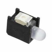
591-2304-013F Dialight, 591-2304-013F Datasheet
591-2304-013F
Specifications of 591-2304-013F


Related parts for 591-2304-013F


591-2304-013F Summary of contents
Page 1
Features 18 Mbit Density (512K x 36) ■ 550 MHz Clock for High Bandwidth ■ 2-word Burst for reducing Address Bus Frequency ■ Double Data Rate (DDR) Interfaces ■ (data transferred at 1100 MHz) at 550 MHz Available in 2.5 ...
Page 2
Logic Block Diagram (CY7C21701KV18 (17:0) Address Register LD K CLK K Gen. DOFF V REF Control R/W Logic BWS [3:0] Document Number: 001-57344 Rev. *A Write Write Reg Reg Output Logic Control Read Data Reg Reg. ...
Page 3
Contents Features............................................................................. 1 Configurations .................................................................. 1 Functional Description..................................................... 1 Logic Block Diagram (CY7C21701KV18)........................ 2 Contents ............................................................................ 3 Pin Configuration ............................................................. 4 165-Ball FBGA ( 1.4 mm) Pinout .................. 4 Pin Definitions .................................................................. 5 Functional Overview ........................................................ 7 ...
Page 4
Pin Configuration The pin configuration for CY7C21701KV18 follows NC/144M NC/36M B NC DQ27 DQ18 DQ28 D NC DQ29 DQ19 DQ20 F NC DQ30 DQ21 G NC DQ31 DQ22 H ...
Page 5
Pin Definitions Pin Name I/O DQ Input Output- Data Input Output Signals. Inputs are sampled on the rising edge of K and K clocks during valid write [35:0] Synchronous operations. These pins drive out the requested data when the read ...
Page 6
Pin Definitions (continued) Pin Name I/O TDO Output TDO for JTAG. TCK Input TCK Pin for JTAG. TDI Input TDI Pin for JTAG. TMS Input TMS Pin for JTAG. NC N/A Not Connected to the Die. Can be tied to ...
Page 7
Functional Overview The CY7C21701KV18 are synchronous pipelined Burst SRAMs equipped with a DDR interface, which operates with a read latency of two and half cycles when DOFF pin is tied HIGH. When DOFF pin is set LOW or connected to ...
Page 8
Valid Data Indicator (QVLD) QVLD is provided on the DDR II+ to simplify data capture on high speed systems. The QVLD is generated by the DDR II+ device along with data output. This signal is also edge aligned with the ...
Page 9
Truth Table The truth table for the CY7C21701KV18 follows. Operation Write Cycle: Load address; wait one cycle; input write data on consecutive K and K rising edges. Read Cycle: (2.5 cycle Latency) Load address; wait two and half cycles; read ...
Page 10
IEEE 1149.1 Serial Boundary Scan (JTAG) These SRAMs incorporate a serial boundary scan Test Access Port (TAP) in the FBGA package. This part is fully compliant with IEEE Standard #1149.1-2001. The TAP operates using JEDEC standard 1.8V I/O logic levels. ...
Page 11
IDCODE The IDCODE instruction loads a vendor-specific, 32-bit code into the instruction register. It also places the instruction register between the TDI and TDO pins and shifts the IDCODE out of the device when the TAP controller enters the Shift-DR ...
Page 12
TAP Controller State Diagram The state diagram for the TAP controller follows. TEST-LOGIC 1 RESET 0 1 TEST-LOGIC/ 0 IDLE Note 11. The 0/1 next to each state represents the value at TMS at the rising edge of TCK. Document ...
Page 13
TAP Controller Block Diagram Selection TDI Circuitry TCK TMS TAP Electrical Characteristics [12, 13, 14] Over the Operating Range Parameter Description V Output HIGH Voltage OH1 V Output HIGH Voltage OH2 V Output LOW Voltage OL1 V Output LOW Voltage ...
Page 14
TAP AC Switching Characteristics [15, 16] Over the Operating Range Parameter t TCK Clock Cycle Time TCYC t TCK Clock Frequency TF t TCK Clock HIGH TH t TCK Clock LOW TL Setup Times t TMS Setup to TCK Clock ...
Page 15
Identification Register Definitions Instruction Field Revision Number (31:29) Cypress Device ID (28:12) Cypress JEDEC ID (11:1) ID Register Presence (0) Scan Register Sizes Register Name Instruction Bypass ID Boundary Scan Instruction Codes Instruction Code EXTEST 000 IDCODE 001 SAMPLE Z ...
Page 16
Boundary Scan Order Bit # Bump ID Bit # 11P 37 10 ...
Page 17
Power Up Sequence in DDR II+ SRAM DDR II+ SRAMs must be powered up and initialized in a predefined manner to prevent undefined operations. Power Up Sequence Apply power and drive DOFF either HIGH or LOW (All other ■ inputs ...
Page 18
Maximum Ratings Exceeding maximum ratings may impair the useful life of the device. These user guidelines are not tested. Storage Temperature .................................. -65°C to +150°C Ambient Temperature with Power Applied... -55°C to +125°C Supply Voltage on V Relative to GND ...
Page 19
Electrical Characteristics (continued) DC Electrical Characteristics [14] Over the Operating Range Parameter Description [21] V Operating Supply Automatic Power down SB1 Current AC Electrical Characteristics [13] Over the Operating Range Parameter Description V Input HIGH Voltage ...
Page 20
Capacitance Tested initially and after any design or process change that may affect these parameters. Parameter Description C Input Capacitance IN C Output Capacitance O Thermal Resistance Tested initially and after any design or process change that may affect these ...
Page 21
Switching Characteristics [22, 23] Over the Operating Range Cypress Consortium Parameter Parameter t V (Typical) to the First Access POWER Clock Cycle Time CYC KHKH t t Input Clock (K/K) HIGH KH KHKL t t Input ...
Page 22
Switching Waveforms Read/Write/Deselect Sequence Figure 5. Waveform for 2.5 Cycle Read Latency NOP READ READ CYC KHKH R ...
Page 23
Ordering Information The following table contains only the parts that are currently available. If you do not see what you are looking for, contact your local sales representative. For more information, visit the Cypress website at http://www.cypress.com/products Cypress maintains a ...
Page 24
Document History Page Document Title: CY7C21701KV18, 18-Mbit DDR II+ SRAM 2-Word Burst Architecture (2.5 Cycle Read Latency) with ODT Document Number: 001-57344 Orig. of Submission Rev. ECN Change ** 2798874 VKN/AESA 11/04/09 *A 2888780 NJY 03/08/2010 Sales, Solutions, and Legal ...