LE ATB S2W-JW-1+LBMB-24+G OSRAM Opto Semiconductors Inc, LE ATB S2W-JW-1+LBMB-24+G Datasheet
LE ATB S2W-JW-1+LBMB-24+G
Specifications of LE ATB S2W-JW-1+LBMB-24+G
Q65110A8183


Related parts for LE ATB S2W-JW-1+LBMB-24+G


LE ATB S2W-JW-1+LBMB-24+G Summary of contents
Page 1
... OSTAR - SMT Lead (Pb) Free Product - RoHS Compliant LE ATB S2W Vorläufige Daten / Preliminary Data Besondere Merkmale • Gehäusetyp: Kompakte Lichtquelle in Multi-Chip SMT Technologie mit Glasabdeckung • Besonderheit des Bauteils: extrem hohe Helligkeit und Leuchtdichte dank Oberflächenemission und niedrigem R • Wellenlänge: 617 nm (amber); 525 nm (true green) ...
Page 2
... In a similar manner for colors where wavelength groups are measured and binned, single wavelength groups will be shipped on any one reel. E.g. LE ATB S2W-JW-1+LBMB-24+GWHW-23 means that only 1 wavelength group -2, - will be shippable. In order to ensure availability, single wavelength groups will not be orderable (see page 5 for explanation). ...
Page 3
... Sperrspannung pro Chip DC Reverse voltage per chip =25°C) S 2009-03-17 Symbol Symbol amber stg (min.) F (max not designed for reverse ATB S2W Werte Einheit Values Unit true blue green – 40 … °C – 40 … °C 125 °C 100 mA 1000 mA 2000 mA V operation ...
Page 4
... (typ (max.) F (max η (typ.) opt (typ.) A Color (typ Φ (typ.) v, 120 R th JSP 4 LE ATB S2W Werte Values amber true blue green 617 525 465 613 515 458 617 529 464 625 533 470 120 2.1 2.9 2.5 3.6 3 ...
Page 5
... Brightness Group Wavelength true green Seite 20 Lichtstärke Luminous Intensity Ι (cd (typ.) 43 (typ.) 55 (typ.) 70 (typ.) 6 (typ.) 10 (typ.) blue max. min. max. 521 458 464 527 464 470 533 Helligkeitsgruppe Brightness Group blue GW LE ATB S2W 1) page 20 Einheit Unit Wellenlänge Wavelength 2 ...
Page 6
... Relative Spectral Emission per Chip λ spektrale Augenempfindlichkeit / Standard eye response curve Φ λ ° 700 mA rel A F 100 % Φ rel 400 450 2009-03-17 2) Seite 20 2) page 20 V blue λ amber true green 500 550 6 LE ATB S2W OHL04115 600 650 nm 700 λ ...
Page 7
... Relativer zonaler Lichtstromanteil 2) page 20 Relative Partial flux ϕ Φ Φ (90° ° 2009-03-17 30˚ 20˚ 10˚ 0.8 0.6 0.4 2) Seite ATB S2W 0˚ 1.0 0.8 0.6 0.4 0.2 0 0˚ 20˚ 40˚ 60˚ 80˚ OHL03736 100˚ 120˚ ...
Page 8
... Forward Current per chip OHL02681 V 3 Relativer Lichtstrom Relative Luminous Flux Φ /Φ V OHL12619 Seite 20 2) page °C; true green; blue 2.0 2.5 3.0 3 Seite page 20 true green; blue (700 mA ° Φ V Φ V (700 mA ATB S2W 4 OHL02613 blue true green ...
Page 9
... Seite 20 Dominante Wellenlänge 2) page 20 Dominant Wavelength Δλ °C; true green dom F A 2009-03-17 Dominante Wellenlänge 2) page 20 Dominant Wavelength λ °C; blue dom ATB S2W 2) Seite 20 ...
Page 10
... F Relative Vorwärtsspannung pro Chip Relative Forward Voltage per chip ΔV (25 ° 700 mA 2009-03-17 2) Seite 20 2) page 20 amber 2) Seite 20 Relative Vorwärtsspannung pro Chip 2) page 20 Relative Forward Voltage per chip ΔV true green = ATB S2W 2) page 20 blue (25 ° 700 mA Seite 20 ...
Page 11
... Seite 20 Relative Lichtstrom 2) page 20 Relative Luminous Flux Φ /Φ (25 ° 700 mA Seite 20 Relative Lichtstrom 2) page 20 Relative Luminous Flux Φ /Φ (25 ° 700 mA 2009-03-17 amber Relative Lichtstrom Relative Luminous Flux Φ /Φ true green ATB S2W 2) Seite 20 2) page 20 blue (25 ° 700 mA ...
Page 12
... Seite 20 Dominante Wellenlänge 2) page 20 Dominant Wavelength Δλ 700 mA; amber dom Seite 20 Dominante Wellenlänge 2) page 20 Dominant Wavelength Δλ 700 mA; true green dom j F 2009-03-17 Dominante Wellenlänge 2) page 20 Dominant Wavelength Δλ 700 mA; blue dom ATB S2W 2) Seite 20 ...
Page 13
... Maximal zulässiger Durchlassstrom Max. Permissible Forward Current for blue chip operated F S 2009-03-17 Maximal zulässiger Durchlassstrom Max. Permissible Forward Current for 2 true green chips operated F S Maximal zulässiger Durchlassstrom Max. Permissible Forward Current for 4 chips operated ATB S2W ...
Page 14
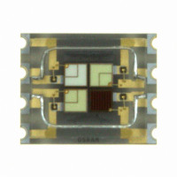
... Maßzeichnung 6) page 20 Package Outlines Chip-Position: 1: amber 2: true green 3: blue 4: true green Gewicht / Approx. weight: 2009-03-17 Pin-Assignment: P1: Cathode; Chip 1 P2: Anode; Chip 1 P3: Cathode; Chip 2 P4: Anode; Chip 2 P5: Cathode; Chip 3 P6: Anode; Chip 3 P7: Cathode; Chip 4 P8: Anode; Chip ATB S2W ...
Page 15
... Seite 20 Verpackung 6) page 20 Method of Packing Elektrisches Ersatzschaltbild Equivalent Circuit Diagram 2009-03-17 500 St. pro Rolle = Verpackungseinheit 500 pcs. per reel = packing unit 15 LE ATB S2W ...
Page 16
... Vorbehandlung nach JEDEC Level 2 Preconditioning acc. to JEDEC Level 2 (nach J-STD-020B) (acc. to J-STD-020B) Maximum Solder Profile Recommended Solder Profile Minimum Solder Profile 120 s max 100 150 16 LE ATB S2W 6) Seite 20 6) page 20 OHLA0687 +0 ˚C 260 ˚C -5 ˚C 245 ˚C ±5 ˚C +5 ˚C 235 ˚C -0 ˚ ...
Page 17
... Forward Voltage Group Wavelength Group Brightness Group OHA12043 Label Direction of unreeling Gurtvorlauf: 400 mm Leader: 400 mm Gurtende: 160 mm Trailer: 160 1.5 + 0.1 1.75 ± 0.1 (0.059 + 0.004) (0.069 ± 0.004) LE ATB S2W OHAY0324 F 5.5 ± 0.05 (0.217 ± 0.002 max 18.4 (0.724) ...
Page 18
... If dry. adequately desiccant change still parts 5% wet, If MIL-I-8835 Indicator Humidity Desiccant Barcode label Länge / length 200 ±5 (7,874 ±0,1968 ATB S2W Humidity indicator Barcode label OHA00539 Barcode label Packing Sealing label Höhe / height 30 ±5 (1,1811 ±0,1968) OHA02044 ...
Page 19
... Components used in life-support devices or systems must be expressly authorized for such purpose! Critical 10) page 20 components may only be used in life-support devices or systems OS. 2009-03-17 11) page 20 with the express written approval of OSRAM 19 LE ATB S2W Date of change 2008-11-13 2009-03-03 2009-03-17 ...
Page 20
... Life support devices or systems are intended ( implanted in the human body, or (b) to support and/or maintain and sustain human life. If they fail reasonable to assume that the health and the life of the user may be endangered. LE ATB S2W ...