HFBR-1528 Avago Technologies US Inc., HFBR-1528 Datasheet - Page 5
HFBR-1528
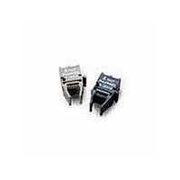
Manufacturer Part Number
HFBR-1528
Description
XMITTER OPT HI PERFORMANCE HORZ
Manufacturer
Avago Technologies US Inc.
Datasheet
1.HFBR-2528.pdf
(8 pages)
Specifications of HFBR-1528
Wavelength
650nm
Spectral Bandwidth
21nm
Voltage - Forward (vf) Typ
2.1V
Current - Dc Forward (if)
60mA
Voltage - Dc Reverse (vr) (max)
3V
Capacitance
60pF
Connector Type
Versatile Link
Function
High Preformance Link Transmitter, High Voltage Transient, Reduces Voltage Transient Susceptibility.
Product
Transmitter
Data Rate
40 MBd
Diode Capacitance
60 pF
Maximum Rise Time
13 ns
Maximum Fall Time
10 ns
Operating Supply Voltage
4.75 V to 5.25 V
Maximum Operating Temperature
+ 85 C
Minimum Operating Temperature
- 40 C
For Use With
Plastic Optical Fiber
Lead Free Status / RoHS Status
Lead free / RoHS Compliant
Available stocks
Company
Part Number
Manufacturer
Quantity
Price

Company:
Part Number:
HFBR-1528Z
Manufacturer:
AVAGO
Quantity:
784


Electrical and Optical Characteristics:
Notes:
1. Typical data are at +25°C, V
2. Input power levels are for peak (not average) optical input levels. For 50% duty cycle data, peak optical power is twice the average optical
3. Receiver overdrive (P
4. Typical value measured from junction to PC board solder joint for horizontal mount package, HFBR-2528.
5. Pins 5 and 8 are electrically connected to the conductive housing and are also used for mounting and retaining purposes. It is required that
6. In recommended receiver circuit, with an optical signal from the recommended transmitter circuit.
7. Pin 4 is electrically isolated internally. Pin 4 may be externally connected to pin 1 for board layout compatibility with HFBR-25X1, HFBR-25X2
8. BER ≤ 10E-9, includes a 10.8 dB margin below the receiver switching threshold level (signal to noise ratio = 12).
HFBR-2528 Receiver
The HFBR-2528 receiver consists of
a silicon PIN photodiode and digitiz-
ing IC to produce a logic compatible
output. The IC includes a unique
circuit to correct the pulse width
distortion of the first bit after a long
idle period. This enables operation
from DC to 10 MBd with low PWD
5
Peak POF Sensitivity:
Minimum Input for
Logic “0”
Peak POF Overdrive
Limit:Maximum
Input for Logic “0”
Peak POF Off State
Limit: Maximum
Input for Logic “1”
Peak HCS
Sensitivity: Minimum
Input for Logic “0”
Peak HCS Overdrive
Limit: Maximum
Input for Logic “0”
Peak HCS Off State
Limit: Maximum
Input for Logic “1”
Supply Current
High Level Output
Voltage
Low Level Output
Voltage
Output Rise Time
Output Fall Time
Thermal Resistance,
Junction to Case
Electric Field
Immunity
Power Supply
Noise Immunity
power.
cal powers above P
formance at high received optical powers.
pins 5 and 8 be connected to ground to maintain conductive housing shield effectiveness.
and HFBR-25X4. Otherwise it is recommended pin 4 be grounded as in Figure 5.
Parameter
RL,max
RL,max
. However, it may not meet a 30% symbol period PWD if the overdrive limit is exceeded. Refer to Figure 2 for PWD per-
) is specified as the limit where |PWD| will not exceed 30 ns. The receiver will be in the correct state (logic “0”) for opti-
CC
= 5.0 V.
Symbol
P
P
P
P
P
P
PSNI
E
RH,max
RH,max
V
RL,max
RL,max
RL,min
RL,min
V
I
θ
MAX
t
t
CC
OL
OH
r
f
jc
+1.0
+0.0
Min.
-1.0
-1.0
-2.0
-3.0
T
4.2
0.1
A
= -40° to +85°C, 4.75 V < V
for arbitrary data patterns.
The receiver output is a “push-pull”
stage compatible with TTL and
CMOS logic. The receiver housing is
a dark, conductive plastic, compat-
ible with all Versatile Link connec-
tors.
-23.0
-25.0
Typ
+5.0
+3.0
0.22
200
4.7
0.4
27
12
10
8
.[1]
-21.0
-20.0
-19.5
-23.0
-22.0
-21.5
Max.
-42
-44
0.4
45
30
30
CC
°C/W
dBm
dBm
dBm
dBm
dBm
dBm
V/m
Unit
mA
V
ns
ns
< 5.25 V, unless otherwise noted.
V
V
pp
-40 to +85
-40 to +85
-40 to +85
-40 to +85
0 to +70
0 to +70
0 to +70
0 to +70
T
+25
+25
+25
+25
A
(°C)
HFBR-2528 Receiver, Top View
GROUND 5
GROUND 8
1 mm POF,
|PWD| < 30 ns
1 mm POF,
|PWD| < 30 ns
1 mm POF
200 µm HCS,
|PWD| < 30 ns
200 µm HCS,
|PWD| < 30 ns
200 µm HCS
V
I
I
C
C
Near Field,
Electrical
Field Source
Sine Wave
DC - 10 MHz
O
O
O
L
L
= -40 µA
= +1.6 mA
Condition
= Open
= 10 pF
= 10 pF
HFBR-2528 Receiver
SEE NOTES 5,7
IC
Note
2,3,
2,6,
2,3,
2,6,
2,6
2,6
6
8
6
8
6
6
4
5
6
4
3
2
1
NO CONNECT
V
GROUND
V
CC
O
1,2,
Fig.
2,4
3
Related parts for HFBR-1528
Image
Part Number
Description
Manufacturer
Datasheet
Request
R

Part Number:
Description:
FIBER OPTIC CBL SIMPLEX 1=100M
Manufacturer:
Avago Technologies US Inc.
Datasheet:

Part Number:
Description:
FIBER OPTIC CBL SIMPLEX 1=500M
Manufacturer:
Avago Technologies US Inc.
Datasheet:

Part Number:
Description:
FIBER OPTIC CONN LATCH GRY SIMPL
Manufacturer:
Avago Technologies US Inc.
Datasheet:

Part Number:
Description:
FIBER OPTIC CONN LATCH BLU SIMPL
Manufacturer:
Avago Technologies US Inc.
Datasheet:

Part Number:
Description:
XMITTER VERSATILE LINK HORZ
Manufacturer:
Avago Technologies US Inc.
Datasheet:

Part Number:
Description:
Fiber Optic Transmitters, Receivers, Transceivers 1300nm 155MBd 16-pin DIP ST Rx
Manufacturer:
Avago Technologies US Inc.

Part Number:
Description:
FIBER OPTIC CBL DUPLEX 1=100M
Manufacturer:
Avago Technologies US Inc.
Datasheet:
Part Number:
Description:
FIBER OPTIC CBL SIMPLEX 1=500M
Manufacturer:
Avago Technologies US Inc.
Datasheet:
Part Number:
Description:
FIBER OPTIC CBL DUPLEX 1=500M
Manufacturer:
Avago Technologies US Inc.
Datasheet:

Part Number:
Description:
FIBER OPTIC CBL SIMPLEX 1=100M
Manufacturer:
Avago Technologies US Inc.
Datasheet:

Part Number:
Description:
OPTOCOUPLER GATE DRV 2A 16-SOIC
Manufacturer:
Avago Technologies US Inc.
Datasheet:
Part Number:
Description:
OPTOCOUPLER 2CH 2.5A 16-SOIC
Manufacturer:
Avago Technologies US Inc.
Datasheet:

Part Number:
Description:
OPTOCOUPLER GATE DRV 0.4A 16SOIC
Manufacturer:
Avago Technologies US Inc.
Datasheet:

Part Number:
Description:
OPTOCOUPLER 2.0A 250KHZ 8-DIP
Manufacturer:
Avago Technologies US Inc.
Datasheet:

Part Number:
Description:
OPTOCOUPLER 2.0A 250KHZ GW 8-SMD
Manufacturer:
Avago Technologies US Inc.
Datasheet: