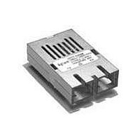
HFCT-5208M Avago Technologies US Inc., HFCT-5208M Datasheet - Page 4

HFCT-5208M
Manufacturer Part Number
HFCT-5208M
Description
TXRX 1X9 622MBIT/S SONET/SDH ATM
Manufacturer
Avago Technologies US Inc.
Datasheet
1.HFBR-5000.pdf
(20 pages)
Specifications of HFCT-5208M
Data Rate
622Mbps
Wavelength
1300nm
Applications
General Purpose
Voltage - Supply
4.75 V ~ 5.25 V
Connector Type
SC
Mounting Type
Through Hole
Function
Designed for implement a range of solutions for ATM/SONET STS-12/SDH, STM-4 Application.
Product
Transceiver
Maximum Rise Time
0.51 ns, 1.25 ns
Maximum Fall Time
0.51 ns, 1.25 ns
Pulse Width Distortion
0.04 ns
Maximum Output Current
50 mA
Operating Supply Voltage
4.75 V to 5.25 V
Maximum Operating Temperature
+ 70 C
Minimum Operating Temperature
0 C
Package / Case
SIP-9
For Use With
Singlemode Glass
Lead Free Status / RoHS Status
Contains lead / RoHS non-compliant
Figure 4. Recommended Circuit Schematic for dc Coupling (at +5 V) between Optical Transceiver and Physical Layer IC
Recommended Circuit Schematic
When designing the HFBR/HFCT-5208M circuit interface,
there are a few fundamental guidelines to follow. For
example, in the Recommended Circuit Schematic, Figure
4, the differential data lines should be treated as 50 ohm
Microstrip or stripline transmission lines. This will help to
minimize the parasitic inductance and capacitance effects.
Proper termination of the differential data signal will prevent
reflections and ringing which would compromise the signal
fidelity and generate unwanted electrical noise. Locate
termination at the received signal end of the transmission
line. The length of these lines should be kept short and of
equal length to prevent pulse-width distortion from
occurring. For the high-speed signal lines, differential signals
should be used, not single-ended signals. These differential
signals need to be loaded symmetrically to prevent
unbalanced currents from flowing which will cause
distortion in the signal.
4
TERMINATION
AT PHY
DEVICE
INPUTS
MOUNTING POST
NO INTERNAL CONNECTION
V
Rx
R6
EER
1
RD
R5
RD
2
V
CC
C6
RD
RD
R7
3
R8
HFBR/HFCT-5208M
SD
SD
4
C7
TOP VIEW
R10
R9
C1
TRANSCEIVER
AT V
V
C3
Rx
V
5
CCR
CC
L1
V
FILTER
CC
CC
PINS
V
Tx
NO INTERNAL CONNECTION
CCT
C4
6
L2
C2
TD
7
TD
MOUNTING POST
TERMINATION
AT TRANSCEIVER
INPUTS
R1
TD
R2
8
In addition to these recommenda-tions, Avago
Technolgies’ Application Engineering staff is available for
consulting on best layout practices with various vendors’
serializer/deserializer, clock recovery/generation integrated
circuits.
Reference Design
Avago Technolgies has developed a reference design for
multimode and single-mode OC-12 ATM-SONET/SDH
applications shown in Figure 6. This reference design uses
a Vitesse Semiconductor Inc.’s VSC8117 clock recovery/
clock generation/serializer/deserializer integrated circuit and
a PMC-Sierra Inc. PM5355 framer IC. Application Note 1178
documents the design, layout, testing and performance of
this reference design. Gerber files, schematic and
application note are available from the Avago Technolgies
web site at the URL of http://www.avagotech.com
V
CC
V
Tx
C5
R3
EET
9
R4
TD
NOTES:
THE SPLIT-LOAD TERMINATIONS FOR PECL
SIGNALS NEED TO BE LOCATED AT THE INPUT
OF DEVICES RECEIVING THOSE PECL SIGNALS.
RECOMMEND MULTI-LAYER PRINTED CIRCUIT
BOARD WITH 50 OHM MICROSTRIP OR
STRIPLINE SIGNAL PATHS BE USED.
R1 = R4 = R6 = R8 = R10 = 130 OHMS.
R2 = R3 = R5 = R7 = R9 = 82 OHMS.
C1 = C2 = C3 = C5 = C6 = 0.1 F.
C4 = C7 = 10 F.
L1 = L2 = 1 H COIL OR FERRITE
INDUCTOR (see text comments).


