AFCT-5963NGZ Avago Technologies US Inc., AFCT-5963NGZ Datasheet - Page 6
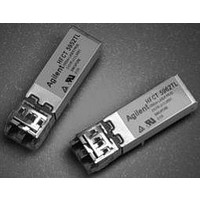
AFCT-5963NGZ
Manufacturer Part Number
AFCT-5963NGZ
Description
TXRX OPT SM SONET OC3/SDH 2X5
Manufacturer
Avago Technologies US Inc.
Series
METRAKr
Datasheet
1.AFCT-5963TGZ.pdf
(16 pages)
Specifications of AFCT-5963NGZ
Applications
General Purpose
Data Rate
155Mbps
Wavelength
1300nm
Voltage - Supply
3.1 V ~ 3.5 V
Connector Type
LC Duplex
Mounting Type
Through Hole
Data Rate Max
0.155Gbps
Supply Voltage
3.3V
Wavelength Typ
1300nm
Leaded Process Compatible
Yes
Optical Fiber Type
TX/RX
Data Transfer Rate
155Mbps
Optical Rise Time
2/2.2ns
Optical Fall Time
2/2.2ns
Operating Temperature Classification
Commercial
Peak Wavelength
1360nm
Package Type
DIP With Connector
Operating Supply Voltage (min)
3.1V
Operating Supply Voltage (typ)
3.3V
Operating Supply Voltage (max)
3.5V
Output Current
50mA
Operating Temp Range
-5C to 70C
Mounting
Snap Fit To Panel
Pin Count
10
Lead Free Status / RoHS Status
Lead free / RoHS Compliant
Lead Free Status / RoHS Status
Lead free / RoHS Compliant, Lead free / RoHS Compliant


Connection Diagram
Figure 5. Pin Out Diagram (Top View)
Pin Descriptions:
Pin 1 Receiver Signal Ground V
Directly connect this pin to the receiver ground
plane.
Pin 2 Receiver Power Supply V
Provide +3.3 V dc via the recommended receiver
power supply filter circuit. Locate the power
supply filter circuit as close as possible to the
V
cause V
Pin 3 Signal Detect SD:
Normal optical input levels to the receiver
result in a logic “1” output.
Low optical input levels to the receiver result
in a logic “0” output.
This Signal Detect output can be used to drive
a +3.3 V TTL input on an upstream circuit,
such as Signal Detect input or Loss of Signal-
bar.
Pin 4 Receiver Data Out Bar RD-:
No internal terminations are provided. See
recommended circuit schematic.
Pin 5 Receiver Data Out RD+:
No internal terminations are provided. See
recommended circuit schematic.
6
CC
RX pin. Note: the filter circuit should not
CC
to drop below minimum specification.
RECEIVER SIGNAL GROUND
RECEIVER POWER SUPPLY
RECEIVER DATA OUT BAR
CC
EE
RECEIVER DATA OUT
RX:
RX:
SIGNAL DETECT
o
o
o
o
o
RX
1
2
3
4
5
View
Top
10
Pin 6 Transmitter Power Supply
V
Provide +3.3 V dc via the recommended
transmitter power supply filter circuit. Locate
the power supply filter circuit as close as
possible to the V
Pin 7 Transmitter Signal Ground
V
Directly connect these pins to the transmitter
signal ground plane.
Pin 8 Transmitter Disable T
Optional feature, connect this pin to +3.3 V
TTL logic high “1” to disable module. To enable
module connect to TTL logic low “0”.
Pin 9 Transmitter Data In TD+:
No internal terminations are provided. See
recommended circuit schematic.
Pin 10 Transmitter Data In Bar TD-:
No internal terminations are provided. See
recommended circuit schematic.
Mounting Studs/Solder Posts
TX
9
8
7
6
CC
EE
o
o
o
o
o
TX:
TX:
TRANSMITTER DATA IN BAR
TRANSMITTER DATA IN
TRANSMITTER DISABLE
TRANSMITTER SIGNAL GROUND
TRANSMITTER POWER SUPPLY
Mounting Studs/
Solder Posts
CC
TX pin.
DIS
:
Related parts for AFCT-5963NGZ
Image
Part Number
Description
Manufacturer
Datasheet
Request
R

Part Number:
Description:
TXRX OPT 1X9 155MB/S 1300NM BK
Manufacturer:
Avago Technologies US Inc.
Datasheet:

Part Number:
Description:
TXRX OPT SFF PLUGGABLE BAIL
Manufacturer:
Avago Technologies US Inc.
Datasheet:
Part Number:
Description:
TXRX OPT SFF PLUGGABLE BAIL DMI
Manufacturer:
Avago Technologies US Inc.
Datasheet:

Part Number:
Description:
TXRX 125MBD DUPLEX BLACK SC 1X9
Manufacturer:
Avago Technologies US Inc.
Datasheet:
Part Number:
Description:
TXRX 125MBD DUPLEX BLUE SC 1X9
Manufacturer:
Avago Technologies US Inc.
Datasheet:

Part Number:
Description:
TXRX OPT SM 155MBS SONET OC3/SDH
Manufacturer:
Avago Technologies US Inc.
Datasheet:
Part Number:
Description:
TXRX SFF SM OC3/STM-1 BAIL DMI
Manufacturer:
Avago Technologies US Inc.
Datasheet:
Part Number:
Description:
TXRX 125MBD DUPLEX BLACK SC 1X9
Manufacturer:
Avago Technologies US Inc.
Datasheet:
Part Number:
Description:
TXRX 125MBD DUPLEX BLUE SC 1X9
Manufacturer:
Avago Technologies US Inc.
Datasheet:

Part Number:
Description:
TXRX OPT SM 155MBS SONET OC3/SDH
Manufacturer:
Avago Technologies US Inc.
Datasheet:

Part Number:
Description:
OPTOCOUPLER GATE DRV 2A 16-SOIC
Manufacturer:
Avago Technologies US Inc.
Datasheet:
Part Number:
Description:
OPTOCOUPLER 2CH 2.5A 16-SOIC
Manufacturer:
Avago Technologies US Inc.
Datasheet:

Part Number:
Description:
OPTOCOUPLER GATE DRV 0.4A 16SOIC
Manufacturer:
Avago Technologies US Inc.
Datasheet:

Part Number:
Description:
OPTOCOUPLER 2.0A 250KHZ 8-DIP
Manufacturer:
Avago Technologies US Inc.
Datasheet:

Part Number:
Description:
OPTOCOUPLER 2.0A 250KHZ GW 8-SMD
Manufacturer:
Avago Technologies US Inc.
Datasheet: