AFCT-5611Z Avago Technologies US Inc., AFCT-5611Z Datasheet - Page 8
AFCT-5611Z
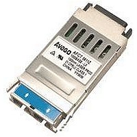
Manufacturer Part Number
AFCT-5611Z
Description
TXRX 1.25GBD GBIC PLUGGABLE
Manufacturer
Avago Technologies US Inc.
Datasheet
1.AFBR-5601Z.pdf
(13 pages)
Specifications of AFCT-5611Z
Applications
Ethernet
Data Rate
1.25Gbd
Wavelength
1310nm
Voltage - Supply
4.75 V ~ 5.25 V
Connector Type
GBIC
Mounting Type
Panel Mount
Supply Voltage
5V
Wavelength Typ
850nm
Peak Reflow Compatible (260 C)
Yes
Leaded Process Compatible
Yes
Optical Fiber Type
TX/RX
Optical Rise Time
0.26/0.35ns
Optical Fall Time
0.26/0.35ns
Jitter
0.227ns
Operating Temperature Classification
Commercial
Peak Wavelength
860nm
Operating Supply Voltage (min)
4.75V
Operating Supply Voltage (typ)
5V
Operating Supply Voltage (max)
5.25V
Operating Temp Range
0C to 60C
Pin Count
20
Lead Free Status / RoHS Status
Lead free / RoHS Compliant
Lead Free Status / RoHS Status
Lead free / RoHS Compliant, Lead free / RoHS Compliant


Short Wavelength GBIC: AFBR-5601Z
Transmitter Section
The transmitter section consists of an 850 nm VCSEL in
an optical subassembly (OSA), which mates to the fiber
cable. The VCSEL OSA is driven by a custom, silicon bi-
polar IC which converts differential logic signals into an
analog Laser Diode drive current.
Receiver Section
The receiver includes a GaAs PIN photodiode mounted
together with a custom, silicon bipolar transimpedance
preamplifier IC, in an OSA. The OSA interfaces to a cus-
tom silicon bipolar circuit that provides post-amplifica-
tion and quantization. The post-amplifier includes a
Signal Detect circuit that provides TTL compatible logic-
low output in response to the detection of a usable input
optical signal.
Absolute Maximum Ratings
Stresses in excess of the absolute maximum ratings can cause catastrophic damage to the device. Limits apply to each
parameter in isolation, all other parameters having values within the recommended operating conditions. It should not
be assumed that limiting values of more than one parameter can be applied to the product at the same time. Exposure
to the absolute maximum ratings for extended periods can adversely affect device reliability.
Recommended Operating Conditions
Transceiver Electrical Characteristics
(T
Notes:
1. Up to applied V
2. See Figure 1 for measurement point.
3. Maximum current is specified at V
4. Hot plug above actual steady state current.
5. Total T
8
Parameter
Storage Temperature
Supply Voltage
Data Input Voltage
TransmitterDifferential Input Voltage
Relative Humidity
Parameter
Ambient Operating Temperature
Case Temperature
Supply Voltage
Supply Current
Parameter
Surge Current
Power Dissipation
A
= 0°C to +60°C, V
X
+ R
X
.
DD
T.
CC
= 4.75 V to 5.25 V)
CC
= maximum @ maximum operating temperature and end of life.
Symbol
T
V
V
TX_DAT
±TX_DAT
RH
Symbol
T
T
V
V
I
Symbol
I
P
TX
SURGE
A
S
CASE
DD
DD
DD
DD
DISS
+ I
T
T
R
R
RX
Eye Safety Design
The laser driver is designed to be Class 1 eye safe
(CDRH21 CFR(J), IEC 60825-1) under a single fault condi-
tion. To be eye safe, only one of two results can occur in
the event of a single fault. The transmitter must either
maintain normal eye safe operation or the transmitter
should be disabled.
There are three key elements to the safety circuitry: a
monitor diode, a window detector circuit, and direct
control of the laser bias. The window detection circuit
monitors the average optical power using the monitor
diode. If a fault occurs such that the dc regulation circuit
cannot maintain the preset bias conditions within ±20%,
the transmitter will automatically be disabled. Once this
has occurred, an electrical power reset will allow an at-
tempted turn-on of the transmitter. TX_FAULT can also
be cleared by cycling TX_DISABLE high for a time interval
>10 µs.
Min.
-40
-0.5
-0.5
5
Min.
0
4.75
Min.
Typ.
Typ.
5.0
200
Typ.
1.00
Max.
+85
6.0
V
2000
95
Max.
+60
+75
5.25
300
Max.
+30
1.58
DD
T
Unit
°C
V
V
mV p-p
%
Unit
°C
°C
V
mA
Unit
mA
W
Notes
1
Notes
2
3
Notes
4
5
Related parts for AFCT-5611Z
Image
Part Number
Description
Manufacturer
Datasheet
Request
R

Part Number:
Description:
TXRX OPT 1X9 155MB/S 1300NM BK
Manufacturer:
Avago Technologies US Inc.
Datasheet:

Part Number:
Description:
TXRX OPT SFF PLUGGABLE BAIL
Manufacturer:
Avago Technologies US Inc.
Datasheet:
Part Number:
Description:
TXRX OPT SFF PLUGGABLE BAIL DMI
Manufacturer:
Avago Technologies US Inc.
Datasheet:

Part Number:
Description:
TXRX 125MBD DUPLEX BLACK SC 1X9
Manufacturer:
Avago Technologies US Inc.
Datasheet:
Part Number:
Description:
TXRX 125MBD DUPLEX BLUE SC 1X9
Manufacturer:
Avago Technologies US Inc.
Datasheet:

Part Number:
Description:
TXRX OPT SM 155MBS SONET OC3/SDH
Manufacturer:
Avago Technologies US Inc.
Datasheet:
Part Number:
Description:
TXRX SFF SM OC3/STM-1 BAIL DMI
Manufacturer:
Avago Technologies US Inc.
Datasheet:
Part Number:
Description:
TXRX 125MBD DUPLEX BLACK SC 1X9
Manufacturer:
Avago Technologies US Inc.
Datasheet:
Part Number:
Description:
TXRX 125MBD DUPLEX BLUE SC 1X9
Manufacturer:
Avago Technologies US Inc.
Datasheet:

Part Number:
Description:
TXRX OPT SM 155MBS SONET OC3/SDH
Manufacturer:
Avago Technologies US Inc.
Datasheet:

Part Number:
Description:
OPTOCOUPLER GATE DRV 2A 16-SOIC
Manufacturer:
Avago Technologies US Inc.
Datasheet:
Part Number:
Description:
OPTOCOUPLER 2CH 2.5A 16-SOIC
Manufacturer:
Avago Technologies US Inc.
Datasheet:

Part Number:
Description:
OPTOCOUPLER GATE DRV 0.4A 16SOIC
Manufacturer:
Avago Technologies US Inc.
Datasheet:

Part Number:
Description:
OPTOCOUPLER 2.0A 250KHZ 8-DIP
Manufacturer:
Avago Technologies US Inc.
Datasheet:

Part Number:
Description:
OPTOCOUPLER 2.0A 250KHZ GW 8-SMD
Manufacturer:
Avago Technologies US Inc.
Datasheet: