AFCT-5963TGZ Avago Technologies US Inc., AFCT-5963TGZ Datasheet - Page 6
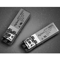
AFCT-5963TGZ
Manufacturer Part Number
AFCT-5963TGZ
Description
TXRX OPT SM SONET OC3/SDH 2X5
Manufacturer
Avago Technologies US Inc.
Series
METRAKr
Datasheet
1.AFCT-5963TGZ.pdf
(16 pages)
Specifications of AFCT-5963TGZ
Applications
General Purpose
Data Rate
155Mbps
Wavelength
1300nm
Voltage - Supply
3.1 V ~ 3.5 V
Connector Type
LC Duplex
Mounting Type
Through Hole
Data Rate Max
0.155Gbps
Supply Voltage
3.3V
Wavelength Typ
1300nm
Leaded Process Compatible
Yes
Lead Free Status / RoHS Status
Lead free / RoHS Compliant


Connection Diagram
Figure 5. Pin Out Diagram (Top View)
Pin Descriptions:
Pin 1 Receiver Signal Ground V
Directly connect this pin to the receiver ground
plane.
Pin 2 Receiver Power Supply V
Provide +3.3 V dc via the recommended receiver
power supply filter circuit. Locate the power
supply filter circuit as close as possible to the
V
cause V
Pin 3 Signal Detect SD:
Normal optical input levels to the receiver
result in a logic “1” output.
Low optical input levels to the receiver result
in a logic “0” output.
This Signal Detect output can be used to drive
a +3.3 V TTL input on an upstream circuit,
such as Signal Detect input or Loss of Signal-
bar.
Pin 4 Receiver Data Out Bar RD-:
No internal terminations are provided. See
recommended circuit schematic.
Pin 5 Receiver Data Out RD+:
No internal terminations are provided. See
recommended circuit schematic.
6
CC
RX pin. Note: the filter circuit should not
CC
to drop below minimum specification.
RECEIVER SIGNAL GROUND
RECEIVER POWER SUPPLY
RECEIVER DATA OUT BAR
CC
EE
RECEIVER DATA OUT
RX:
RX:
SIGNAL DETECT
o
o
o
o
o
RX
1
2
3
4
5
View
Top
10
Pin 6 Transmitter Power Supply
V
Provide +3.3 V dc via the recommended
transmitter power supply filter circuit. Locate
the power supply filter circuit as close as
possible to the V
Pin 7 Transmitter Signal Ground
V
Directly connect these pins to the transmitter
signal ground plane.
Pin 8 Transmitter Disable T
Optional feature, connect this pin to +3.3 V
TTL logic high “1” to disable module. To enable
module connect to TTL logic low “0”.
Pin 9 Transmitter Data In TD+:
No internal terminations are provided. See
recommended circuit schematic.
Pin 10 Transmitter Data In Bar TD-:
No internal terminations are provided. See
recommended circuit schematic.
Mounting Studs/Solder Posts
TX
9
8
7
6
CC
EE
o
o
o
o
o
TX:
TX:
TRANSMITTER DATA IN BAR
TRANSMITTER DATA IN
TRANSMITTER DISABLE
TRANSMITTER SIGNAL GROUND
TRANSMITTER POWER SUPPLY
Mounting Studs/
Solder Posts
CC
TX pin.
DIS
:
Related parts for AFCT-5963TGZ
Image
Part Number
Description
Manufacturer
Datasheet
Request
R

Part Number:
Description:
TXRX OPT 1X9 155MB/S 1300NM BK
Manufacturer:
Avago Technologies US Inc.
Datasheet:

Part Number:
Description:
TXRX OPT SFF PLUGGABLE BAIL
Manufacturer:
Avago Technologies US Inc.
Datasheet:
Part Number:
Description:
TXRX OPT SFF PLUGGABLE BAIL DMI
Manufacturer:
Avago Technologies US Inc.
Datasheet:

Part Number:
Description:
TXRX 125MBD DUPLEX BLACK SC 1X9
Manufacturer:
Avago Technologies US Inc.
Datasheet:
Part Number:
Description:
TXRX 125MBD DUPLEX BLUE SC 1X9
Manufacturer:
Avago Technologies US Inc.
Datasheet:

Part Number:
Description:
TXRX OPT SM 155MBS SONET OC3/SDH
Manufacturer:
Avago Technologies US Inc.
Datasheet:
Part Number:
Description:
TXRX SFF SM OC3/STM-1 BAIL DMI
Manufacturer:
Avago Technologies US Inc.
Datasheet:
Part Number:
Description:
TXRX 125MBD DUPLEX BLACK SC 1X9
Manufacturer:
Avago Technologies US Inc.
Datasheet:
Part Number:
Description:
TXRX 125MBD DUPLEX BLUE SC 1X9
Manufacturer:
Avago Technologies US Inc.
Datasheet:

Part Number:
Description:
TXRX OPT SM 155MBS SONET OC3/SDH
Manufacturer:
Avago Technologies US Inc.
Datasheet:

Part Number:
Description:
OPTOCOUPLER GATE DRV 2A 16-SOIC
Manufacturer:
Avago Technologies US Inc.
Datasheet:
Part Number:
Description:
OPTOCOUPLER 2CH 2.5A 16-SOIC
Manufacturer:
Avago Technologies US Inc.
Datasheet:

Part Number:
Description:
OPTOCOUPLER GATE DRV 0.4A 16SOIC
Manufacturer:
Avago Technologies US Inc.
Datasheet:

Part Number:
Description:
OPTOCOUPLER 2.0A 250KHZ 8-DIP
Manufacturer:
Avago Technologies US Inc.
Datasheet:

Part Number:
Description:
OPTOCOUPLER 2.0A 250KHZ GW 8-SMD
Manufacturer:
Avago Technologies US Inc.
Datasheet: