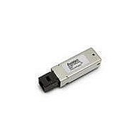
AFBR-5905EZ Avago Technologies US Inc., AFBR-5905EZ Datasheet - Page 2

AFBR-5905EZ
Manufacturer Part Number
AFBR-5905EZ
Description
TXRX ATM/SONET OC-3 2X5
Manufacturer
Avago Technologies US Inc.
Datasheet
1.AFBR-5905Z.pdf
(13 pages)
Specifications of AFBR-5905EZ
Wavelength
1308nm
Data Rate
*
Applications
General Purpose
Voltage - Supply
3.135 V ~ 3.465 V
Connector Type
MTRJ
Mounting Type
Through Hole
Function
MMC OC-3 PB-Free MTRFJ
Product
Transceiver
Maximum Rise Time
3 ns, 2.2 ns
Maximum Fall Time
3 ns, 2.2 ns
Pulse Width Distortion
0.21 ns, 0.15 ns
Maximum Output Current
50 mA
Operating Supply Voltage
3.135 V to 3.465 V
Maximum Operating Temperature
+ 70 C
Minimum Operating Temperature
0 C
For Use With
Multimode Glass
Lead Free Status / RoHS Status
Lead free / RoHS Compliant
Receiver Sections
The receiver section of the AFBR-5905Z utilizes an InGaAs
PIN photodiode coupled to a custom silicon transimped-
ance preamplifier IC. It is packaged in the optical sub-
assembly portion of the receiver. This PIN/preamplifier
combination is coupled to a custom quantizer IC which
provides the final pulse shaping for the logic output and
the Signal Detect function. The Data output is differen-
tial. The Signal Detect output is singleended. Both Data
and Signal Detect outputs are PECL compatible, ECL ref-
erenced (shifted) to a 3.3 V power supply. The receiver
outputs, Data Out and Data Out Bar, are squelched at Sig-
nal Detect Deassert. That is, when the light input power
decreases to a typical -38 dBm or less, the Signal Detect
Deasserts, i.e. the Signal Detect output goes to a PECL low
state. This forces the receiver outputs, Data Out and Data
Out Bar to go to steady PECL levels High and Low respec-
tively.
Package
The overall package concept for the Avago transceiver
consists of three basic elements; the two optical subas-
semblies, an electrical subassembly, and the housing as
illustrated in the block diagram in Figure 1.
The package outline drawing and pin out are shown in
Figures 2 and 3. The details of this package outline and pin
out are compliant with the multisource definition of the
2
are squelched at Signal Detect
Deassert. That is, when the
light input power decreases to
a typical -38 dBm or less, the
Signal Detect Deasserts, i.e. the
Signal Detect output goes to a
PECL low state. This forces
the receiver outputs, Data Out
and Data Out Bar to go to
steady PECL levels High and
Low respectively.
Package
The overall package concept
for the Agilent transceiver
consists of three basic
elements; the two optical
subassemblies, an electrical
subassembly, and the housing
as illustrated in the block
diagram in Figure 1.
The package outline drawing
and pin out are shown in
Figures 2 and 3. The details of
Figure 1. Block Diagram.
DATA IN
DATA IN
DATA OUT
DATA OUT
SIGNAL
DETECT
this package outline and pin
out are compliant with the
multisource definition of the 2
x 5 DIP. The low profile of the
Agilent transceiver design
complies with the maximum
height allowed for the MT-RJ
connector over the entire
length of the package.
The optical subassemblies
utilize a high-volume assembly
process together with low-cost
lens elements which result in a
cost-effective building block.
The electrical subassembly
consists of a high volume
multilayer printed circuit
board on which the IC and
various surface-mounted
passive circuit elements are
attached.
The receiver section includes
an internal shield for the
LED DRIVER IC
QUANTIZER IC
R
T
X
X
SUPPLY
SUPPLY
R
T
X
X
GROUND
GROUND
2 x 5 DIP. The low profile of the Avago transceiver design
complies with the maximum height allowed for the MT-RJ
connector over the entire length of the package.
The optical subassemblies utilize a high-volume assembly
process together with low-cost lens elements which result
in a cost-effective building block.
The electrical subassembly consists of a high volume mul-
tilayer printed circuit board on which the IC and various
surface-mounted passive circuit elements are attached.
The receiver section includes an internal shield for the
electrical and optical subassemblies to ensure high im-
munity to external EMI fields.
The outer housing is electrically conductive and is at re-
ciever signal ground potential. The MT-RJ ports is molded
of filled nonconductive plastic to provide mechanical
strength and electrical isolation. The solder posts of the
Avago design are isolated from the internal circuit of the
transceiver.
The transceiver is attached to a printed circuit board with
the ten signal pins and the two solder posts which exit the
bottom of the housing. The two solder posts provide the
primary mechanical strength to withstand the loads im-
posed on the transceiver by mating with the MT-RJ con-
nectored fiber cables.
PIN PHOTODIODE
PRE-AMPLIFIER
SUBASSEMBLY
LED
OPTICAL
SUBASSEMBLY
electrical and optical
subassemblies to ensure high
immunity to external EMI
fields.
The outer housing is
electrically conductive and is
at reciever signal ground
potential. The MT-RJ ports is
molded of filled nonconductive
plastic to provide mechanical
strength and electrical
isolation. The solder posts of
the Agilent design are isolated
from the internal circuit of the
transceiver.
The transceiver is attached to
a printed circuit board with
the ten signal pins and the
two solder posts which exit
the bottom of the housing. The
two solder posts provide the
primary mechanical strength to
withstand the loads imposed
on the transceiver by mating
with the MT-RJ connectored
fiber cables.
MT-RJ
RECEPTACLE


