FTLF8524E2GNL Finisar Corporation, FTLF8524E2GNL Datasheet - Page 6
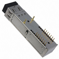
FTLF8524E2GNL
Manufacturer Part Number
FTLF8524E2GNL
Description
TXRX OPT SFF 4 GB/S 850NM
Manufacturer
Finisar Corporation
Type
TX/RXr
Datasheet
1.FTLF8524E2GNL.pdf
(10 pages)
Specifications of FTLF8524E2GNL
Data Rate
4.25Gbps
Wavelength
850nm
Applications
Ethernet
Voltage - Supply
3 V ~ 3.6 V
Connector Type
LC Duplex
Mounting Type
PCB
Package
14SFF
Mounting
Through Hole
Rise Time
0.09/0.12 ns
Jitter
0.119(Max)/0.1224(Max) ns
Operating Supply Voltage
3 to 3.6 V
Lead Free Status / RoHS Status
Lead free / RoHS Compliant
Other names
775-1042
Available stocks
Company
Part Number
Manufacturer
Quantity
Price
Company:

Part Number:
FTLF8524E2GNL
Manufacturer:
FINISAR
Quantity:
65


FTLF8524E2xNy 2x7 Pin SFF Product Specification – July 2005
VIII. Digital Diagnostic Functions
Finisar FTLF8524E2xNy 2x7 SFF transceivers support a 2-wire serial communication
protocol. This interface is identical to the 2-wire serial interface defined in the SFP
4
MSA
, however in this case it is implemented on the 2x7 SFF form factor.
The standard SFP serial ID provides access to identification information that describes
the transceiver’s capabilities, standard interfaces, manufacturer, and other information.
Additionally, an enhanced digital diagnostic monitoring interface is defined, which
allows real-time access to device operating parameters such as transceiver temperature,
laser bias current, transmitted optical power, received optical power and transceiver
supply voltage. It also defines a sophisticated system of alarm and warning flags, which
alerts end-users when particular operating parameters are outside of a factory set normal
range.
In order to access the identification information, the 2x7 SFF transceivers have a 256-
2
byte memory map in E
PROM that is accessible over a 2-wire serial interface at the 8 bit
address 1010000X (A0h). The digital diagnostic monitoring interface makes use of the 8
bit address 1010001X (A2h), so the originally defined serial ID memory map remains
unchanged. The interface is identical to, and is thus fully backward compatible with both
the GBIC Specification and the SFP Multi Source Agreement. Additional information,
including details of the electronic interface, is described in Finisar Application Note AN-
2030: “Digital Diagnostics Monitoring Interface for SFP Optical Transceivers”.
The operating and diagnostics information is monitored and reported by a Digital
Diagnostics Transceiver Controller (DDTC) inside the transceiver, which is accessed
through a 2-wire serial interface. When the serial protocol is activated, the serial clock
signal (SCL, Mod Def 1) is generated by the host. The positive edge clocks data into the
2
2x7 SFF transceiver into those segments of the E
PROM that are not write-protected.
The negative edge clocks data from the 2x7 SFF transceiver. The serial data signal
(SDA, Mod Def 2) is bi-directional for serial data transfer. The host uses SDA in
conjunction with SCL to mark the start and end of serial protocol activation. The
memories are organized as a series of 8-bit data words that can be addressed individually
or sequentially.
4,5
For more information, please see the SFP MSA documentation
and Finisar Application
Note AN-2030.
One difference in the implementation of digital diagnostics in the SFF 2x7 form factor
from the SFP MSA documentation is the readout of Bit 1, Byte 110 at Address A2h
(called “Digital State of the LOS output pin” in the SFP documentation). In the SFF 2x7,
the output of this bit is inverted to indicate Signal Detect and match the output of the
Signal Detect pin on the SFF part.
Digital diagnostics for the FTLF8524E2xNy can be used in host systems that require
either internally or externally calibrated digital diagnostics.
Finisar Corporation July 12, 2005 RevG
Page 6
Related parts for FTLF8524E2GNL
Image
Part Number
Description
Manufacturer
Datasheet
Request
R

Part Number:
Description:
1X9 DWP9F, FLEXGRID, C-BAND, LC CONNECTORS, WAVELENGTH SPACING ENABLES HETE
Manufacturer:
Finisar Corporation
Part Number:
Description:
1X9 DWP50, FIXED 50GHZ CHANNEL SPACING (96CH), C-BAND, LC CONNECTORS
Manufacturer:
Finisar Corporation
Part Number:
Description:
DWDM BROADBAND TUNABLE, 50GHZ SPACING (C-BAND), APD, ITU G.698.1, 10GE, 10G
Manufacturer:
Finisar Corporation
Part Number:
Description:
Power cables for 1RU Power Booster product
Manufacturer:
Finisar Corporation
Part Number:
Description:
1X9 DWP100, 50 OR 100GHZ CHANNEL SPACING (48/96CH), C-BAND, LC CONNECTORS
Manufacturer:
Finisar Corporation
Part Number:
Description:
NRZ-DPSK, UP TO 44.6GB/S TRANSPONDER, VERY LONG HAUL, RX. USING FSR = 66.7G
Manufacturer:
Finisar Corporation
Part Number:
Description:
1550NM EML, PIN, NRZ, OTU3, 43GB/S TRANSPONDER, SINGLE MODE, 300-PIN 3.5X4
Manufacturer:
Finisar Corporation
Part Number:
Description:
C-BAND TUNABLE LASER BUTTERFLY PACKAGE, 89 CHANNELS AT 50 GHZ SPACING FROM
Manufacturer:
Finisar Corporation
Part Number:
Description:
1310NM DFB LC TOSA, 10GBPS, LR
Manufacturer:
Finisar Corporation
Datasheet:
Part Number:
Description:
DWDM CML, 100GHZ SPACING (C-BAND OR L-BAND), OC-192, STM64, 10G FC, G.709
Manufacturer:
Finisar Corporation
Part Number:
Description:
1550NM CML, OC-192, STM-64, 10G FC, G.709, 10.7 GB/S, G.959.1 P1L1 AND P1V1
Manufacturer:
Finisar Corporation
Part Number:
Description:
DWDM CML, 8X50GHZ SPACING (C-BAND OR L-BAND), OC-192, STM-64, 10G FC, G.709
Manufacturer:
Finisar Corporation
Part Number:
Description:
1550NM CML, OC-192, STM-64, 10G FC, G.709, 10.7 GB/S, G.959.1 P1L1 AND P1V1
Manufacturer:
Finisar Corporation
Part Number:
Description:
DWDM CML, 100GHZ SPACING (C-BAND OR L-BAND), OC-192, STM-64, 10G FC, G.709
Manufacturer:
Finisar Corporation
Part Number:
Description:
1550NM CML, OC-192, STM-64, 10G FC, G.709, 10.7 GB/S, G.959.1 P1L1 AND P1V1
Manufacturer:
Finisar Corporation