HFBR-5911LZ Avago Technologies US Inc., HFBR-5911LZ Datasheet - Page 7
HFBR-5911LZ
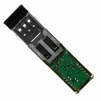
Manufacturer Part Number
HFBR-5911LZ
Description
TXRX OPTICAL SFF 1.25GBD ISCSI
Manufacturer
Avago Technologies US Inc.
Datasheet
1.HFBR-5911LZ.pdf
(12 pages)
Specifications of HFBR-5911LZ
Applications
Ethernet
Data Rate
1.25Gbd
Wavelength
850nm
Voltage - Supply
3.3V
Connector Type
LC Duplex
Mounting Type
Through Hole
Data Rate Max
1.25Gbps
Supply Voltage
3.3V
Wavelength Typ
850nm
Leaded Process Compatible
Yes
Lead Free Status / RoHS Status
Lead free / RoHS Compliant
Other names
516-2084
Available stocks
Company
Part Number
Manufacturer
Quantity
Price
Company:

Part Number:
HFBR-5911LZ
Manufacturer:
Avago Technologies US Inc.
Quantity:
135
Part Number:
HFBR-5911LZ
Manufacturer:
AVAGO/安华高
Quantity:
20 000


Table 8 - Receiver Optical Characteristics
HFBR-5911LZ
HFBR-5911ALZ
Parameter
Input Optical Power
Stressed Receiver Sensitivity
Stressed Receiver Sensitivity
Contributed Total Jitter
Receive Electrical 3dB Upper Cutoff Frequency
Operating Center Wavelength
Return Loss
Signal Detect Assert Power Level
Signal Detect Deassert Power Level
Signal Detect Hysteresis
Table 9 - Transceiver Timing Characteristics
HFBR-5911LZ
HFBR-5911ALZ
Parameter
Interval between Transmit Disable Assertions
Table 10 - PCB Assembly Process Compatibility
Parameter
Hand Lead Soldering Temperature/Time
Notes:
17. Receiver sensitivity is measured using a worst case extinction ratio penalty while sampling at the center of the eye.
18. Stressed receiver sensitivity is measured using the conformance test signal defined by IEEE 802.3, section 38.6.11. The conformance test signal is
19. The Receive Electrical 3 dB Upper Cutoff Frequency of the receiver is measured using the technique outlined in IEEE 802.3, section 38.6.11.
20. Return Loss is defined as the minimum attenuation (dB) of received optical power for energy reflected back into the optical fiber.
21. With valid 8b/10b encoded data.
22. Time from rising edge of Tx_Disable to when modulated optical output falls below 10% of nominal.
23. Time from falling edge of Tx_Disable to when the modulated optical output rises above 90% of nominal.
24. Time from power on or falling edge of Tx_ Disable to when the modulated optical output rises above 90% of nominal.
25. Time Tx_Disable must be held high to disable transmitter. Measured from leading edge of Tx_Disable to when the modulated optical output falls
26. Time from SD deassert to SD assert.
27. Time from non-SD assert to SD deassert.
Tx Disable Assert Time
Tx Disable Deassert Time
Time to initialize
Tx Disable Pulse Width to Reset
Signal Detect Assert Time
Signal Detect Deassert Time
Wave Soldering and Aqueous Wash
Aqueous Wash Pressure
7
conditioned by applying deterministic jitter and intersymbol interference.
below 10% of nominal.
(T
(T
(T
(T
C
C
C
C
= 0ºC to +70ºC, V
= -10 °C to +85 °C, V
= 0ºC to +70ºC, V
= -10 °C to +85 °C, V
62.5 µm
50 µm
CC
CC
= 3.14 V to 3.47 V)
= 3.14 V to 3.47 V)
CC
CC
= 3.14 V to 3.47 V)
= 3.14 V to 3.47 V)
Symbol
P
TJ
RL
P
P
P
Symbol
SD_on
SD_off
Symbol
l
t_off
t_on
t_init
t_reset
T
T
IN
A
D
A
SOLD
SOLD
C
- P
/t
/t
D
SOLD
SOLD
Minimum
-17
770
12
-30
1.5
Minimum
10
10
Minimum
Typical
850
Typical
Typical
1500
100
100
Maximum
0
-12.5
-13.5
266
0.332
860
-17
Maximum
1.0
300
350
Maximum
+260/10
+260/10
110
Units
dBm avg.
dBm avg.
ps
UI
MHz
nm
dB
dBm avg.
dBm avg.
dB
Units
µs
ms
ms
µs
ms
µs
µs
Units
° C / sec
° C / sec
psi
Reference
17
18
19
Reference
Reference
20
21
21
21
22
23
24
25
26
27
Related parts for HFBR-5911LZ
Image
Part Number
Description
Manufacturer
Datasheet
Request
R

Part Number:
Description:
RECEIVER FIBER OPTIC 600NM 40KBD
Manufacturer:
Avago Technologies US Inc.
Datasheet:

Part Number:
Description:
XMITTER FIBER OPTIC 600NM 5MBD
Manufacturer:
Avago Technologies US Inc.
Datasheet:

Part Number:
Description:
XMITTER FIBER OPTIC 600NM 40KBD
Manufacturer:
Avago Technologies US Inc.
Datasheet:

Part Number:
Description:
XMITTER VERSATILE LINK HORZ
Manufacturer:
Avago Technologies US Inc.
Datasheet:

Part Number:
Description:
XMITTER OPT HI PERFORMANCE VERT
Manufacturer:
Avago Technologies US Inc.
Datasheet:

Part Number:
Description:
TXRX FIBER OPTIC 650NM 10MBAUD
Manufacturer:
Avago Technologies US Inc.
Datasheet:
Part Number:
Description:
TXRX FIBER OPTIC 650NM 10MBAUD
Manufacturer:
Avago Technologies US Inc.
Datasheet:

Part Number:
Description:
FIBER OPTIC TRANSMITTER 660NM
Manufacturer:
Avago Technologies US Inc.
Datasheet:

Part Number:
Description:
KIT EVAL FIBER OPTIC 5MBD
Manufacturer:
Avago Technologies US Inc.
Datasheet:
Part Number:
Description:
KIT EVAL FIBER OPTICS 32MBD
Manufacturer:
Avago Technologies US Inc.
Datasheet:

Part Number:
Description:
KIT EVAL FIBER OPTIC 5MBD
Manufacturer:
Avago Technologies US Inc.
Datasheet:

Part Number:
Description:
125MBd 1300nm FiberOptic Eval Kit
Manufacturer:
Avago Technologies US Inc.
Datasheet:

Part Number:
Description:
DC-5MBd 820nm FiberOptic EvalKit
Manufacturer:
Avago Technologies US Inc.
Datasheet:
Part Number:
Description:
125MBd 820nm FiberOptic Eval Kit
Manufacturer:
Avago Technologies US Inc.
Datasheet:
Part Number:
Description:
DC-5MBd 650nm POF Eval Kit
Manufacturer:
Avago Technologies US Inc.
Datasheet: