CU40025-UW6J Noritake Company Inc, CU40025-UW6J Datasheet - Page 13
CU40025-UW6J
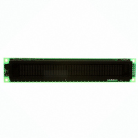
Manufacturer Part Number
CU40025-UW6J
Description
MODULE VF DISPLAY 40X2 5MM CHAR
Manufacturer
Noritake Company Inc
Series
U-Versionr
Specifications of CU40025-UW6J
Outline L X W X H
182.00mm x 33.50mm x 20.50mm
Viewing Area
138.80mm L x 11.50mm W
Display Format
40 x 2
Display Type
Character
Format
5 x 7 Dots
Voltage - Supply
5V
Character Size
4.70mm H x 2.30mm W
Operating Temperature
-40°C ~ 85°C
Resolution
2 X 40
Viewing Area (h X W)
11.5mm X 138.8mm
Supply Current
300mA
Supply Voltage Range
4.75V To 5.25V
Character Format
Dot Matrix
Character Type
5x7 Dot Matrix
External Depth
21mm
External
RoHS Compliant
Product
Character Display Modules
Character Count X Line
40 x 2
Module Size (w X H X T)
182 mm x 33.5 mm x 20.5 mm
Voltage Rating
5 V
Operating Temperature Range
- 40 C to + 85 C
Current Rating
300 mA
Dot Format
5 x 7
Viewing Area (w X H)
138.8 mm x 11.5 mm
Interface
Parallel / Serial
Lead Free Status / RoHS Status
Lead free / RoHS Compliant
Number Of Dots
-
Lead Free Status / Rohs Status
Details
Other names
286-1062
Available stocks
Company
Part Number
Manufacturer
Quantity
Price
Company:

Part Number:
CU40025-UW6J
Manufacturer:
Noritake Company Inc
Quantity:
135


8.3.3 Serial data transfer
Serial data can be inputted when the Strobe goes to “0”.
Serial data consists of 2 bytes. The first byte (Start Byte) consists of a total of 8 bits: the
Synchronous bits (bit1-bit5), R/W (bit6), RS (bit7) and bit8. The register is selected (Instruction
Register or Data Register) by the RS (bit7). RS is “0” in Instruction Register, and it is “1” in
Data Register. The data write or read is selected by R/W (bit6). R/W is “0” when the data is
written, and it is “1” when the data is read.
In “Data Write”, the second byte (8-bit Instruction / Data Byte) is written after the Start Byte.
On the other hand, the second byte is the read data in “Data Read”, such as the Busy Flag +
Address Counter or the data written in the DD RAM or CG RAM. The read data is outputted at
the falling edge of the shift clock.
<Data Write>
<Data Read>
STB
SCK
SI
STB
SCK
1
Synchronous bits
1
1
Synchronous bits
1
2
R/W
1
RS
1
2
3
1
Start Byte
1
3
Start Byte
4
1
Instruction Register
1
4
5
1
Data Write
1
5
R/W
6
R/W
0
6
7
RS
RS
7
8
12
0
0
8
1µs
D7
9
1
BF
D6
Data Register
10
2
Data Read
IR6
Instruction / Data
D5
11
3
1
IR5
Read Data
D4
12
4
IR4
D3
13
5
IR3
D2
14
6
IR2
D1
15
CU40025-UW6J
7
IR1
D0
16
8
IR0
Related parts for CU40025-UW6J
Image
Part Number
Description
Manufacturer
Datasheet
Request
R


Part Number:
Description:
MODULE VF GRAPHIC DISPLAY 112X16
Manufacturer:
Noritake Company Inc
Datasheet:

Part Number:
Description:
MODULE VF DISPLY 16X2 4.8MM CHAR
Manufacturer:
Noritake Company Inc
Datasheet:

Part Number:
Description:
MODULE VF GRAPHIC DISPLAY 140X16
Manufacturer:
Noritake Company Inc
Datasheet:

Part Number:
Description:
MODULE VF DISPLAY 20X2 EXT TEMP
Manufacturer:
Noritake Company Inc
Datasheet:

Part Number:
Description:
MODULE VF DISPLAY 24X2 5MM CHAR
Manufacturer:
Noritake Company Inc
Datasheet:

Part Number:
Description:
MODULE VF GRAPHIC DISPLAY 140X32
Manufacturer:
Noritake Company Inc
Datasheet:

Part Number:
Description:
MODULE VF DISPLAY 24X4 5V CHAR
Manufacturer:
Noritake Company Inc
Datasheet:

Part Number:
Description:
MODULE VF DISPLAY 20X2 5V CHAR
Manufacturer:
Noritake Company Inc
Datasheet:

Part Number:
Description:
MODULE VF DISPLAY 20X2 5V CHAR
Manufacturer:
Noritake Company Inc
Datasheet:

Part Number:
Description:
MODULE VF DISPLAY 24X4 5V CHAR
Manufacturer:
Noritake Company Inc
Datasheet:

Part Number:
Description:
MODULE VF DISP 16X2 8MM CHAR
Manufacturer:
Noritake Company Inc
Datasheet:

Part Number:
Description:
MODULE VF GRAPHIC DISPLAY 140X16
Manufacturer:
Noritake Company Inc
Datasheet:

Part Number:
Description:
MODULE VF DISPLAY 24X6 5V CHAR
Manufacturer:
Noritake Company Inc
Datasheet:

Part Number:
Description:
MODULE VF DISPLAY 24X6 5V CHAR
Manufacturer:
Noritake Company Inc
Datasheet: